Semiconductor package including low temperature co-fired ceramic substrate

a technology of co-fired ceramic and semiconductor elements, which is applied in the direction of semiconductor devices, semiconductor/solid-state device details, electrical devices, etc., can solve the problems of affecting the overall utility of the semiconductor, and the mounting of such semiconductor elements thereto is difficult to control, so as to eliminate the formation of undesirable voids and the effect of a minimal profil

Active Publication Date: 2005-04-12
AMKOR TECH SINGAPORE HLDG PTE LTD
View PDF254 Cites 33 Cited by
  • Summary
  • Abstract
  • Description
  • Claims
  • Application Information

AI Technical Summary

Benefits of technology

In accordance with the present invention, there are provided multiple embodiments of a semiconductor package which each include a low temperature co-fired ceramic substrate. The substrate comprises multiple stacked ceramic layers, and electrically conductive patterns which extend between the layers and along the top surface of the substrate. Disposed on the bottom surface of the substrate are electrode pads which are electrically connected to the conductive patterns through the use of vias. Mounted to the top surface of the substrate are one or more semiconductor dies which are electrically connected to the conductive patterns and to one or more leads extending about the substrate in certain

Problems solved by technology

However, LTCC substrates as currently known in the prior art possess certain deficiencies which detract from their overall utility.
However, in the current LTCC technique, there is a susceptibility of warpage in the panel or strip, which creates problems in the manufacturing process for the semiconductor packages including the LTCC substrate units.
To combat this problem, panels or strips

Method used


Image

  • Semiconductor package including low temperature co-fired ceramic substrate
  • Semiconductor package including low temperature co-fired ceramic substrate
  • Semiconductor package including low temperature co-fired ceramic substrate

Examples


first embodiment

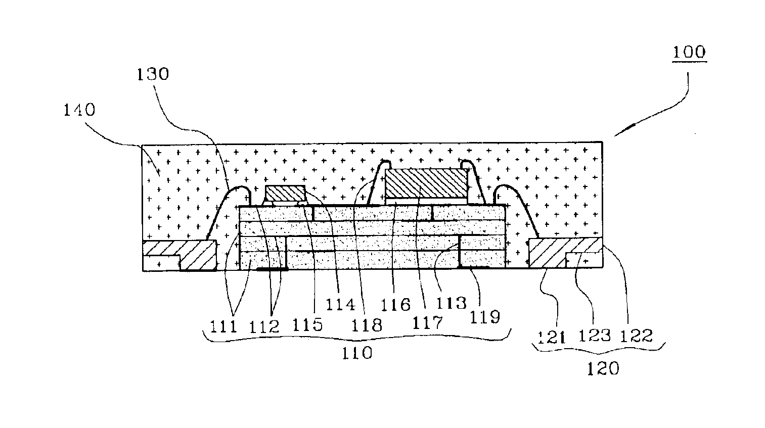
Referring now to the drawings wherein the showings are for purposes of illustrating various embodiments of the present invention only, and not for purposes of limiting the same, FIGS. 1A and 1B illustrate a semiconductor package 100 constructed in accordance with the present invention. The semiconductor package 100 includes a low temperature co-fired ceramic (LTCC) substrate 110 which is a substantially planar plate. More particularly, the LTCC substrate 110 comprises a plurality of stacked ceramic layers 111. Formed on and in between the ceramic layers 111 are a plurality of electrically conductive patterns 112. The conductive patterns 112 formed on and in between the ceramic layers ill are electrically connected to each other through conductive vias 113. As best seen in FIG. 1A, the electrically conductive patterns 112 are included on the top surface of the uppermost ceramic layer 111 of the LTCC substrate 110. Included on the bottom surface of the lowermost ceramic layer 111 in t...

second embodiment

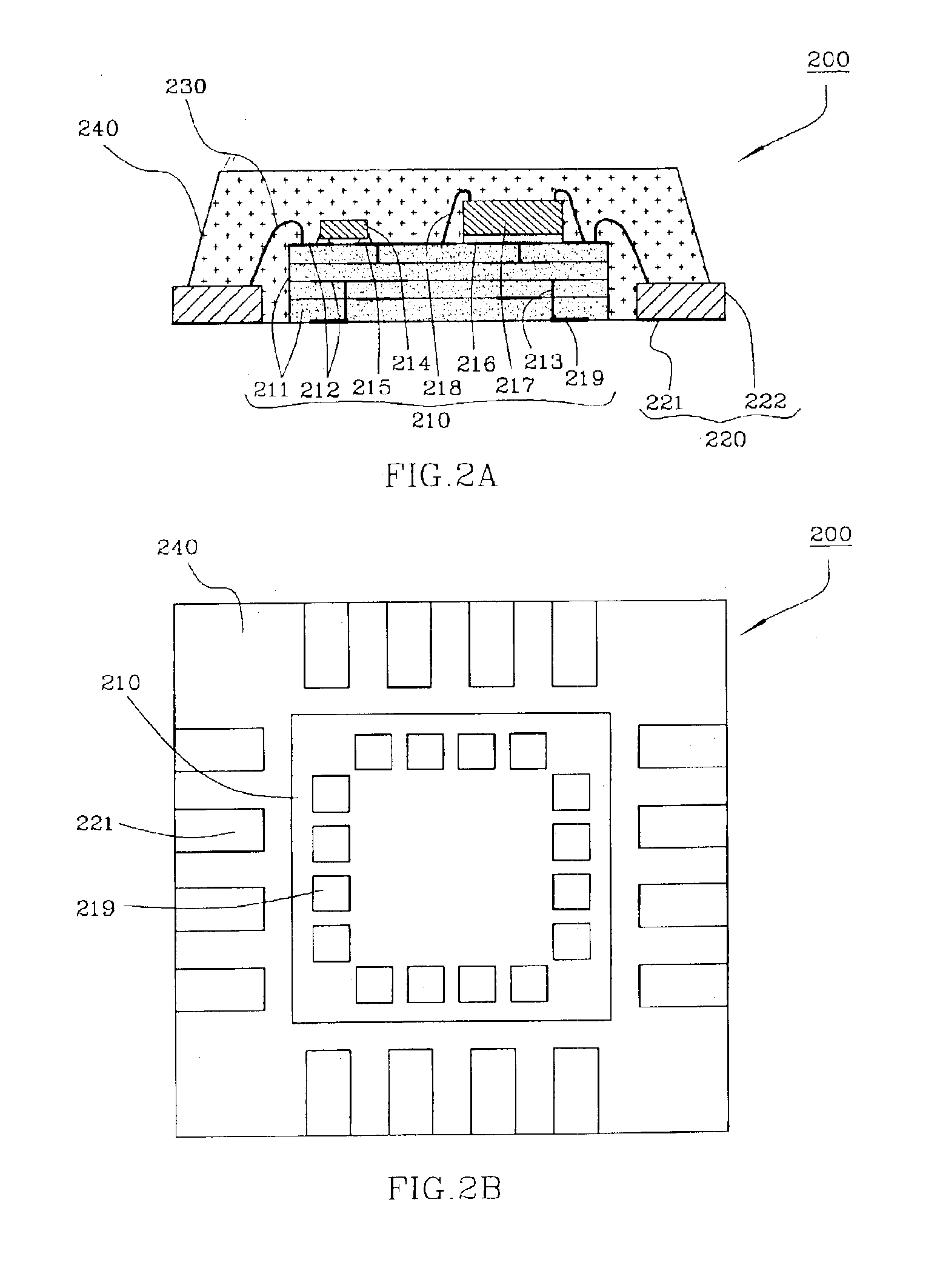
Referring now to FIGS. 2A and 2B, there is shown a semiconductor package 200 constructed in accordance with the present invention. The semiconductor package 200 is substantially similar in structure and function to the above-described semiconductor package 100, with the various elements labeled with the 200 series reference numerals in FIGS. 2A and 2B corresponding to the same elements labeled with the 100 series reference numerals in FIGS. 1A and 1B. The distinctions between the semiconductor package 200 and the semiconductor package 100 lie primarily in the configuration of the leads 220 of the semiconductor package 200 in comparison to the leads 120 of the semiconductor package 100. In this regard, the leads 220 do not include the partially etched surface 123 described above in relation to each of the leads 120. Thus, the entirety of the generally planar bottom surface of each lead 220 defines the electrode pad 221 thereof.

A further distinction between the semiconductor package 2...

fourth embodiment

Referring now to FIGS. 4A and 4B, there is shown a semiconductor package 400 constructed in accordance with the present invention. The semiconductor package 400 is substantially similar in structure and function to the above-described semiconductor package 300, with the elements labeled with the 400 series reference numerals in FIGS. 4A and 4B corresponding to respective ones of the elements labeled with the 300 series reference numerals in FIGS. 3A and 3B. The distinctions between the semiconductor package 400 and the semiconductor package 300 mirror the distinctions between the semiconductor package 200 and the semiconductor package 100. In this regard, in the semiconductor package 400, each of the leads 420 does not include the partially etched surface 323 included in each of the leads 320, thus resulting in the entirety of the generally planar bottom surface of each lead 420 defining the electrode pad 421 thereof. Further, the package body 440 of the semiconductor package 400 ha...


PUM


Abstract

A semiconductor package comprising a low temperature co-fired ceramic substrate defining opposed top and bottom surfaces. The substrate comprises at least two stacked ceramic layers and electrically conductive patterns which extend between the layers and along the top surface of the substrate. Mounted to the top surface of the substrate and electrically connected to the conductive patterns is at least one semiconductor die. A plurality of leads extend at least partially about the substrate in spaced relation thereto. Each of the leads defines opposed top and bottom surfaces, the semiconductor die being electrically connected to at least one of the leads. A package body at least partially encapsulates the substrate, the semiconductor die and the leads such that at least a portion of the bottom surface of each of the leads is exposed in the package body.

Description

CROSS-REFERENCE TO RELATED APPLICATIONS(Not Applicable)STATEMENT RE: FEDERALLY SPONSORED RESEARCH / DEVELOPMENT(Not Applicable)BACKGROUND OF THE INVENTION1. Field of the InventionThe present invention relates generally to semiconductor packages and, more particularly, to a semiconductor package which is fabricated to include a low temperature co-fired ceramic (LTCC) substrate, and is uniquely configured to have a minimal profile while including one or more semiconductor dies and / or passive elements of various size and thickness.2. Description of the Related ArtIn the electronic arts and, more particularly, in the field of image mobile communications, there is an increasing need for various electronic components which are extremely small and light. In addition to the need for discrete component parts which are of decreased size and weight, there is also a need for an increase in wiring density in order to meet certain functional requirements. In order to meet these particular requireme...

Claims


Application Information

Patent Timeline
IPC IPC(8): H01L21/56H01L25/065H01L23/495H01L23/31H01L23/28H01L23/498H01L23/48H01L21/02H01L23/49H01L23/64
CPCH01L21/56H01L21/568H01L23/3107H01L23/49531H01L23/49861H01L23/64H01L24/97H01L25/0655H01L21/561H01L2224/45144H01L24/48H01L2224/48091H01L2224/48227H01L2224/48247H01L2224/4911H01L2224/49175H01L2224/73265H01L2224/97H01L2924/01013H01L2924/01027H01L2924/01029H01L2924/01075H01L2924/01079H01L2924/01082H01L2924/09701H01L2924/19041H01L2924/19042H01L2924/19043H01L2924/19105H01L2924/19107H01L2224/45124H01L24/45H01L2924/01033H01L24/49H01L2224/32225H01L2924/00014H01L2224/85H01L2924/00H01L2924/00012H01L2924/15787H01L24/73H01L2924/181
Inventor YANG, JUN YOUNGLEE, SUN GOOLEE, CHOON HEUNG
Owner AMKOR TECH SINGAPORE HLDG PTE LTD
Why Eureka
Try Eureka