Electronic device and electronic apparatus

a technology of electronic equipment and electronic components, applied in the direction of static indicating devices, identification means, instruments, etc., can solve problems such as efforts to improve the performance of active matrix displays, and achieve the effect of improving the operating performance and reliability of el displays

Inactive Publication Date: 2005-04-12
SEMICON ENERGY LAB CO LTD
View PDF57 Cites 51 Cited by
  • Summary
  • Abstract
  • Description
  • Claims
  • Application Information

AI Technical Summary

Benefits of technology

The present invention makes it possible to improve operating performance and reliability of an EL display by using different TFTs appropriately on the same insulator. The principle of the present invention is characterized in that TFT structures are optimized not only in a pixel portion but also in driving circuit portions for driving the pixel portion.

Problems solved by technology

In such a case, it is difficult to maintain performance requirements of all circuits or elements only with TFTs having the same structure, which can be a serious obstacle to efforts toward improved performance of active matrix displays.

Method used


Image

  • Electronic device and electronic apparatus
  • Electronic device and electronic apparatus
  • Electronic device and electronic apparatus

Examples


embodiment 1

[Embodiment 1]

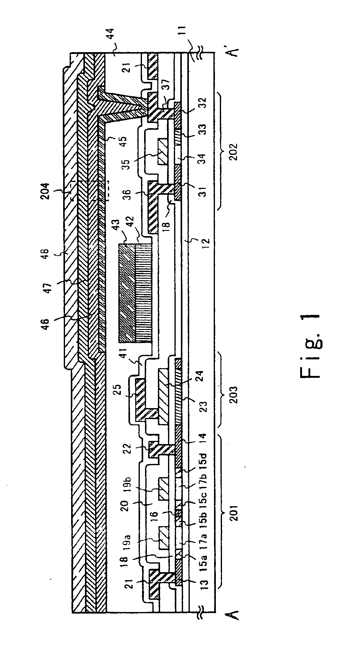
A first embodiment of the invention will be described with reference to FIGS. 3A through 5C. A description will be made here on a method for fabricating TFTs of a pixel portion and driving circuit portions provided around the same simultaneously. For simplicity of the description, only a CMOS circuit is shown which is a basic circuit for such driving circuits.

First, as shown in FIG. 3A, an underlying film 301 having a thickness of 300 nm is formed on a glass substrate 300. In the present embodiment, the a silicon oxinitride film is used as the underlying film 301. At this time, the density of nitrogen in the region in contact with the glass substrate 300 is preferably in the range from 10 to 25 wt %.

Next, an amorphous silicon film (not shown) having a thickness of 50 nm is formed on the underlying film 301 using a known film forming method. The film is not limited to an amorphous silicon film, and it may be any semiconductor film (and any microcrystalline semiconductor...

embodiment 2

[Embodiment 2]

The present embodiment will refer to a case in which a pixel portion of an active matrix EL display has a structure different from that shown in FIG. 1.

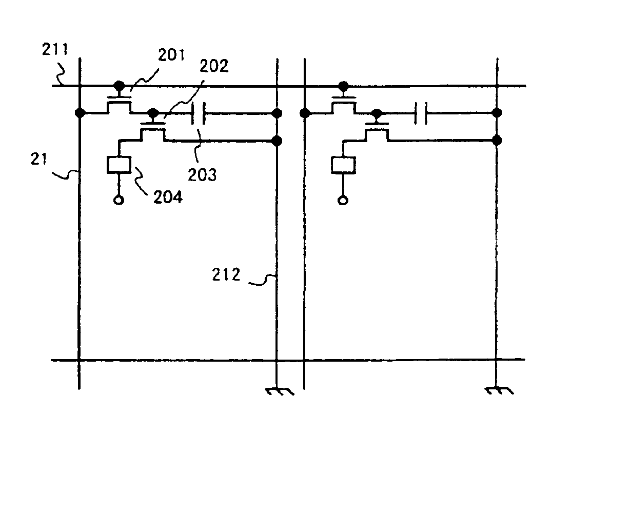
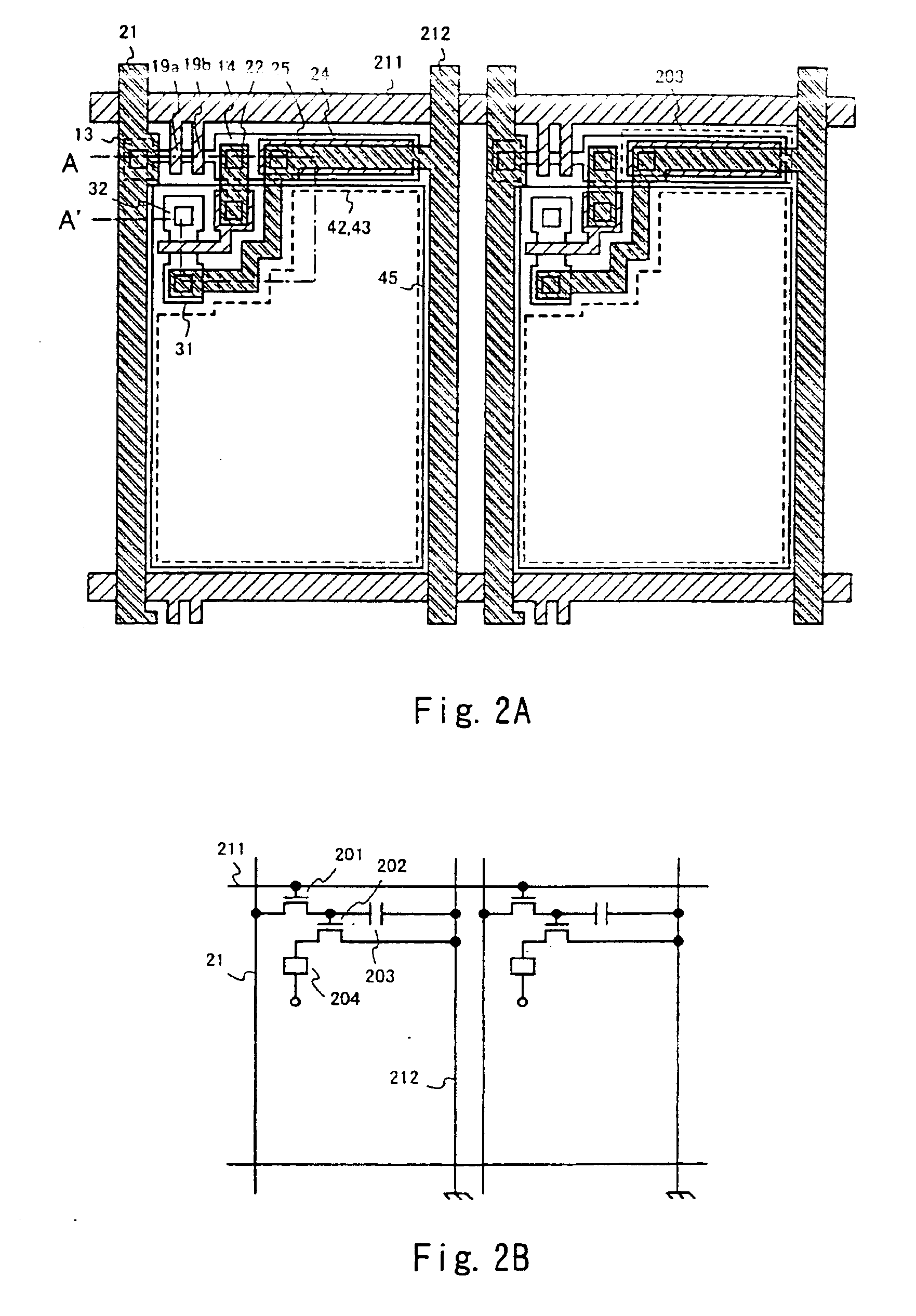
FIG. 6A shows an example of a structure of a switching TFT different from that shown in FIG. 1. A current control TFT 202, storage capacitor 203 and EL element 204 shown in FIG. 6A will not be described because they have completely the same structures as those in the first embodiment. The switching TFT is given new reference numbers only in parts where it is necessary, and the description for FIG. 1 will be used as it is for the remaining parts.

The switching TFT 201 shown in FIG. 1 and the switching TFT 207 shown in FIG. 6A are different in the positions where the LDD regions are formed. While the LDD regions 15a through 15d in FIG. 1 are formed such that they do not overlap the gate electrodes 19a and 19b, the LDD regions of the present embodiment are formed such that they partially overlap gate electrodes.

Specifically...

embodiment 3

[Embodiment 3]

FIG. 7 shows an example of a pixel configuration according to the present embodiment which is different from that shown in FIG. 2B.

In the present embodiment, two pixels as shown in FIG. 2B are provided such that they are symmetric about a current source line 212 for supplying a ground potential. Specifically, as shown in FIG. 7, the current supply line 212 is shard by the two pixels adjacent thereto, which reduces the number of lines required. The structures of the TFTs provided in the pixel and the like may be kept unchanged.

Such a configuration makes it possible to fabricate a pixel portion having higher definition, thereby improving image quality. The configuration according to the present embodiment can be easily implemented according to the fabrication steps of the first embodiment, and the TFT structure may be combined with those in the second embodiment.


PUM


Abstract

An EL display having high operating performance and reliability is provided. LDD regions 15a through 15d of a switching TFT 201 formed in a pixel are formed such that they do not overlap gate electrodes 19a and 19b to provide a structure which is primarily intended for the reduction of an off-current. An LDD region 22 of a current control TFT 202 is formed such that it partially overlaps a gate electrode 35 to provide a structure which is primarily intended for the prevention of hot carrier injection and the reduction of an off-current. Appropriate TFT structures are thus provided depending on required functions to improve operational performance and reliability.

Description

BACKGROUND OF THE INVENTION1. Field of the InventionThe present invention relates to an electronic device formed by fabricating a semiconductor element (element utilizing a semiconductor thin film) on a substrate and an electronic apparatus utilizing such an electronic device as a display portion. Particularly, the present invention is a technique which is advantageously embodied in an active matrix EL (electroluminescence) display which is an electronic device.2. Description of the Related ArtRecently, great advances have been made in techniques for forming TFTs on a substrate, and application of the same to the development of active matrix displays is in progress. Especially, TFTs utilizing polysilicon films are capable of operations at a high speed because they have higher field effect mobility compared to conventional TFTs utilizing amorphous silicon films. This has made it possible to control pixels with a driving circuit formed on the same substrate (insulator) on which the pi...

Claims


Application Information

Patent Timeline
Patent Type & Authority Patents(United States)
IPC IPC(8): H01L27/32H01L29/66H01L27/12H01L27/28H01L21/336H01L21/02H01L29/786H01L51/50G09F9/30H01L21/77H01L27/13H05B33/12H05B33/14H05B44/00
CPCH01L27/124H01L27/3244H01L27/3262H01L27/3265H01L27/3276H01L29/66757H01L29/78621H01L29/78627H01L27/12H01L27/1214H01L27/1255G09G2300/0426G09G2300/0861H01L27/322H01L2251/5315H01L27/13G09G2300/0842H10K59/38H10K59/12H10K59/1213H10K59/1216H10K59/131H10K2102/3026H01L27/1251
Inventor YAMAUCHI, YUKIOFUKUNAGA, TAKESHI
Owner SEMICON ENERGY LAB CO LTD
Why Eureka
Try Eureka