
Memory device array having a pair of magnetic bits sharing a common conductor line

a memory device array and magnetic bit technology, applied in semiconductor devices, digital storage, instruments, etc., can solve the problems of reducing the conductive line only in the way, and the sensing function of the selected memory cell is not accurate,

Inactive Publication Date: 2005-04-12
SAMSUNG ELECTRONICS CO LTD
View PDF11 Cites 76 Cited by
  • Summary
  • Abstract
  • Description
  • Claims
  • Application Information

AI Technical Summary

Benefits of technology

In an alternative embodiment, a data storage device having parallel memory planes is also disclosed. In the alternative embodiment, first there is included a first resistive cross point plane of memory cells and a second resistive cross point plane of memory cells. Further, a word line plane is shared between the first and second planes of memory cells. A plurality of bit lines is provided where each bit line couples one memory cell from the first plane to another memory cell in the second plane. A plurality of unidirectional elements are also provided where each unidirectional element serves to couple one memory cell in either plane wherein the unidirectional elements prevent interference of one memory cell with another memory cell sharing the same bit line.

Problems solved by technology

This action isolates the bit line currents from one another, effectively blocking most of the leakage current that might otherwise flow through secondary paths, possibly causing errors in the sensing function of the selected memory cell.
Several issues relevant to all memory arrays are the need to simplify structures, the desire to increase memory storage density, and the need to reduce conductive lines within the array.
The reduction of conductive lines has been limited to how many cells there are arranged in rows and columns.

Method used


Image

  • Memory device array having a pair of magnetic bits sharing a common conductor line
  • Memory device array having a pair of magnetic bits sharing a common conductor line
  • Memory device array having a pair of magnetic bits sharing a common conductor line

Examples


Embodiment Construction

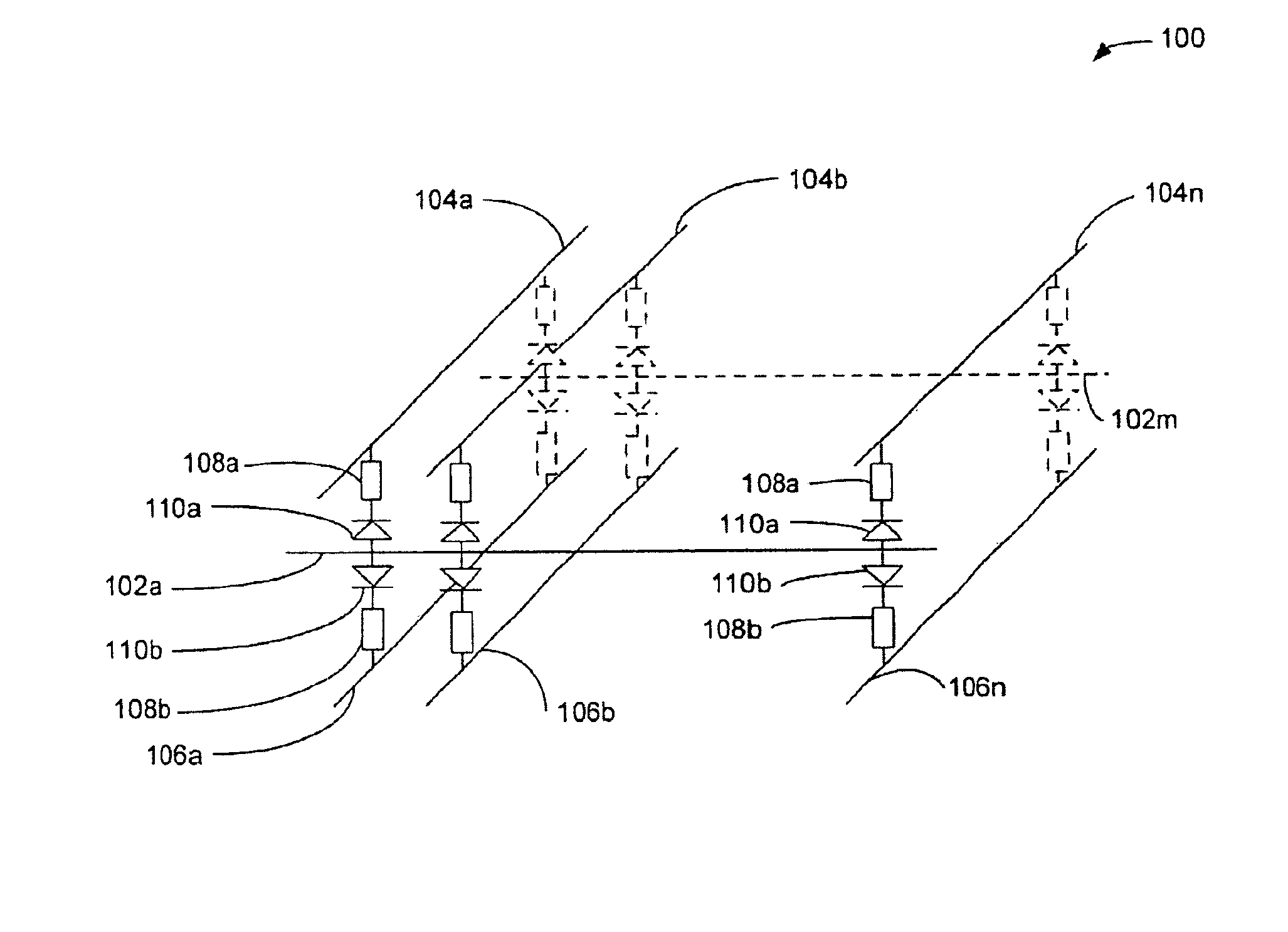
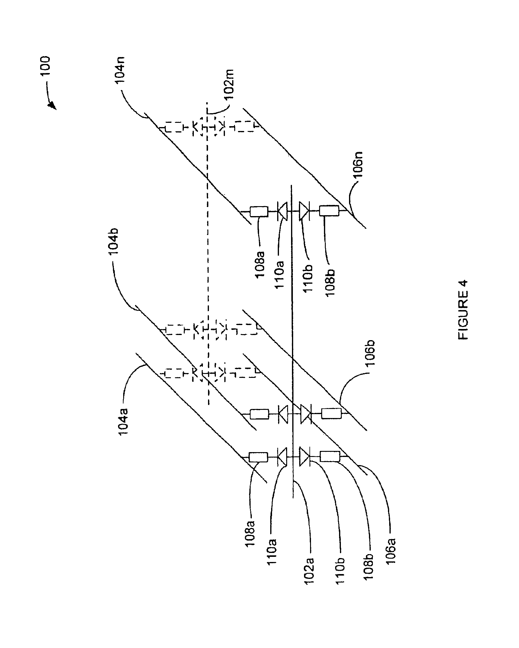
FIG. 4 illustrates an MRAM memory cell array 100 that includes a common word line plane with back-to-back diode memory cell configuration. A three dimensional perspective view illustrates how multiple memory cells are arranged to increase cell density while reducing the number of conductor lines typically required in the prior art. The memory array 100 includes a plurality of row conductor lines 102a-m, each of which serves as a common conductor to memory cells 108a and 108b. Unidirectional conductors 110a and 110b are mated with memory cells 108a and 108b, respectively. The unidirectional switches 110a and 110b enable the common conductor to be active in a manner that only one bit in the bit pair is read, sensed or written to according to the read, sense and write processes described below, without the other cell interfering with the processes.

Memory array 100 further includes a first column conductor line 104 and a second column conductor line 106. A plurality of first column cond...


PUM


Abstract

A data storage device having parallel memory planes is disclosed. Each memory plane includes a first resistive cross point plane of memory cells, a second resistive cross point plane of memory cells, a plurality of conductive word lines shared between the first and second planes of memory cells, a plurality of bit lines, each bit line coupling one or more cells from the first plane to another memory cell in the second plane, and a plurality of unidirectional elements. Further, the one unidirectional element couples a first memory cell from the first plane to a selected word line and a selected bit line in a first conductive direction and a second unidirectional element couples a second cell from the second plane to the selected word line and selected bit line in a second conductive direction. The device further provides for a unidirectional conductive path to form from a memory cell in the first plane to a memory cell in the second plane sharing the same bit line.

Description

BACKGROUND OF THE INVENTIONThe present invention pertains to the field of resistive memory cell arrays. More particularly, this invention relates to a memory array having memory bit pairs sharing a common conductor to increase array density.A resistive random access memory (RAM) is a cross point type memory array of a planar matrix of spaced memory cells sandwiched between two meshes of conductors running in orthogonal directions above and below the cells. An example is the resistive RAM array 10 shown in FIG. 1. The row conductors 12 running in one direction are referred to as the word lines, and the column conductors 14 extending in a second direction usually perpendicular to the first direction are referred to as the bit lines. The memory cells 16 are usually arranged in a square or rectangular array so that each memory cell unit 16 is connected with one word line 12 and an intersecting bit line 14.In a resistive RAM array, the resistance of each memory cell has more than one sta...

Claims


Application Information

Patent Timeline
Patent Type & Authority Patents(United States)
IPC IPC(8): G11C11/16G11C11/02G11C11/15H01L21/8246H01L27/10H01L27/105H01L43/08
CPCG11C11/16G11C11/1659G11C11/1657G11C11/1673H10B61/10G11C11/15
Inventor TRAN, LUNG T.
Owner SAMSUNG ELECTRONICS CO LTD
Features
  • Generate Ideas
  • Intellectual Property
  • Life Sciences
  • Materials
  • Tech Scout
  • Unparalleled Data Quality
  • Higher Quality Content
  • 60% Fewer Hallucinations
Learn More