
Eureka
For R&D, Eureka makes reading and utilizing patents & technical documents easy.
Eureka AIR
Designed for self-driven R&D workflows. Generate viable solutions, solve complex R&D challenges, empower your innovation with AI.

Eureka Materials
Designed for material experts only. Revolutionize your material R&D, from search, analyze, to developing new materials.

TechResearch
Generate reliable direction feasibility study reports for your R&D in just a few steps.

TechSeek
Discover and master advanced knowledge NOW. Basics, ideas, possibilities, all at once.

TechMind
As an expert in R&D Theories, TechMind can generates customized viable solutions instantly.

TechRisk
Analyze your overall solution with one click, know your potential R&D risks in advance.

TechMonitor
Get weekly tech updates, stay abreast of the latest tech innovations and key insights.
Method of forming shallow trench isolation with chamfered corners
- Summary
- Abstract
- Description
- Claims
- Application Information
AI Technical Summary
Benefits of technology
Problems solved by technology
Method used
Image

Examples
Embodiment Construction
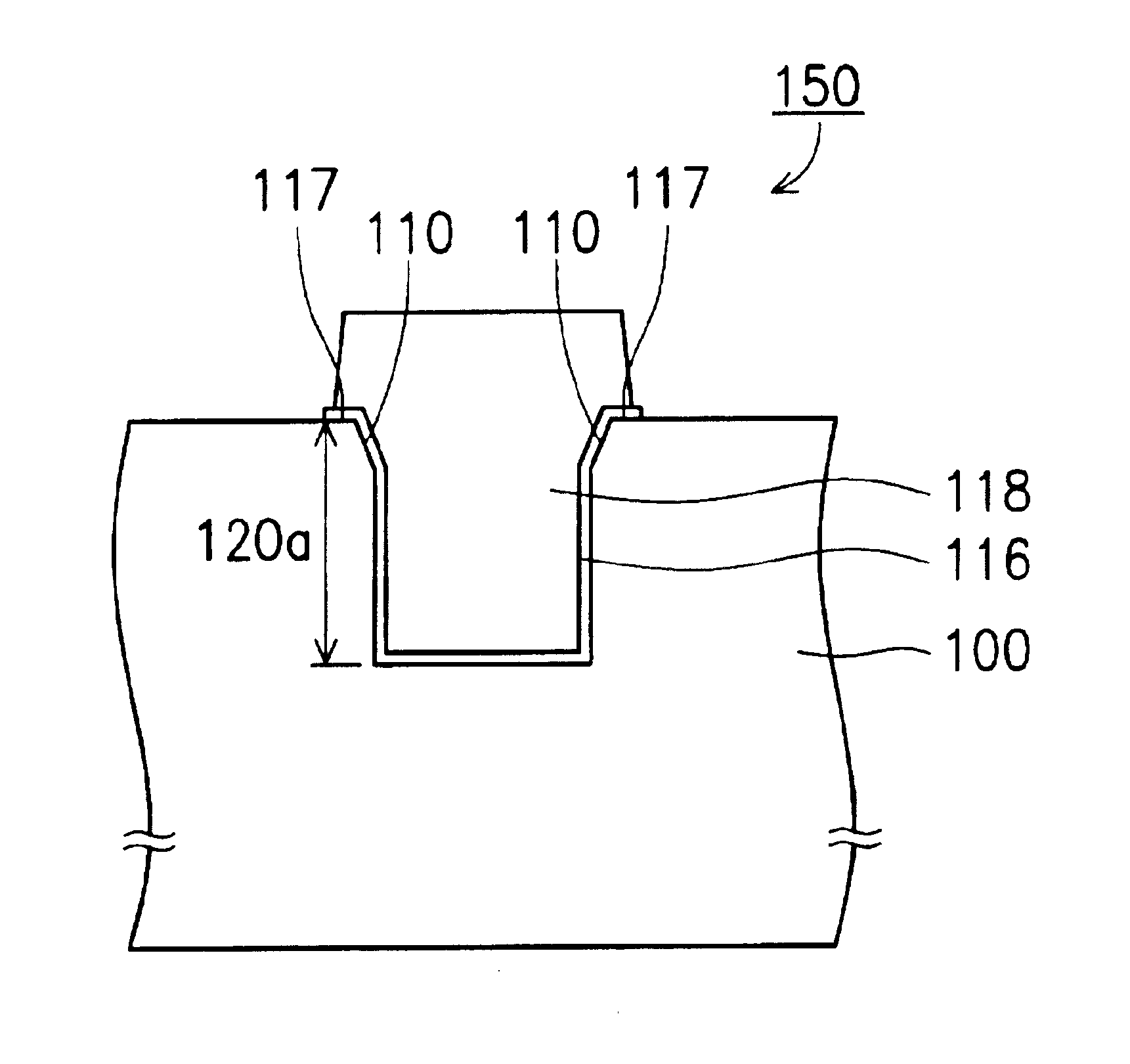
[0029]FIGS. 4A to 4J are cross sections of the manufacturing process of a shallow trench isolation region with chamfered corners in accordance with the present invention.
[0030]First, referring to FIG. 4A, a semiconductor substrate 100, for example silicon substrate, is provided. Herein, use of the term substrate includes devices formed within a semiconductor wafer and the layers overlying the wafer. Next, a pad insulation layer 102, a first mask layer 104 and a second mask layer 106 are formed sequentially on the surface of the semiconductor substrate 100. Preferably, the pad insulation layer 102 such as pad oxide layer with a thickness of 50 Å to 200 Å is formed using thermal oxidation at 850-950° C., APCVD, or LPCVD. The first mask layer 104 such as silicon nitride with a thickness of 5000 Å to 2000 Å is formed using LPCVD at 750-800° C., wherein SiCl2H2 and NH3 are reactants. As well, the first mask layer 104 may also be silicon oxy-nitride formed by LPCVD, wherein SiH4, N2O, and...
PUM
 Abstract
Description
Claims
Application Information
 - R&D Engineer
- R&D Manager
- IP Professional
- Industry Leading Data Capabilities
- Powerful AI technology
- Patent DNA Extraction
Browse by: Latest US Patents, China's latest patents, Technical Efficacy Thesaurus, Application Domain, Technology Topic, Popular Technical Reports.
© 2024 PatSnap. All rights reserved.Legal|Privacy policy|Modern Slavery Act Transparency Statement|Sitemap|About US| Contact US: help@patsnap.com