Light emitting devices for light conversion and methods and semiconductor chips for fabricating the same

a technology of light conversion and light emitting devices, which is applied in the direction of semiconductor devices, basic electric elements, electrical appliances, etc., can solve the problems of limiting the minimum size of a broad spectrum light emitting device and devices may be less than optimal in certain applications, so as to improve light reflection and light conversion.

a technology of light conversion and light emitting devices, which is applied in the direction of semiconductor devices, basic electric elements, electrical appliances, etc., can solve the problems of limiting the minimum size of a broad spectrum light emitting device and devices may be less than optimal in certain applications, so as to improve light reflection and light conversion.

US6885033B2Inactive Publication Date: 2005-04-26CREELED INC

Image

  • Light emitting devices for light conversion and methods and semiconductor chips for fabricating the same
  • Light emitting devices for light conversion and methods and semiconductor chips for fabricating the same
  • Light emitting devices for light conversion and methods and semiconductor chips for fabricating the same

Examples


Embodiment Construction

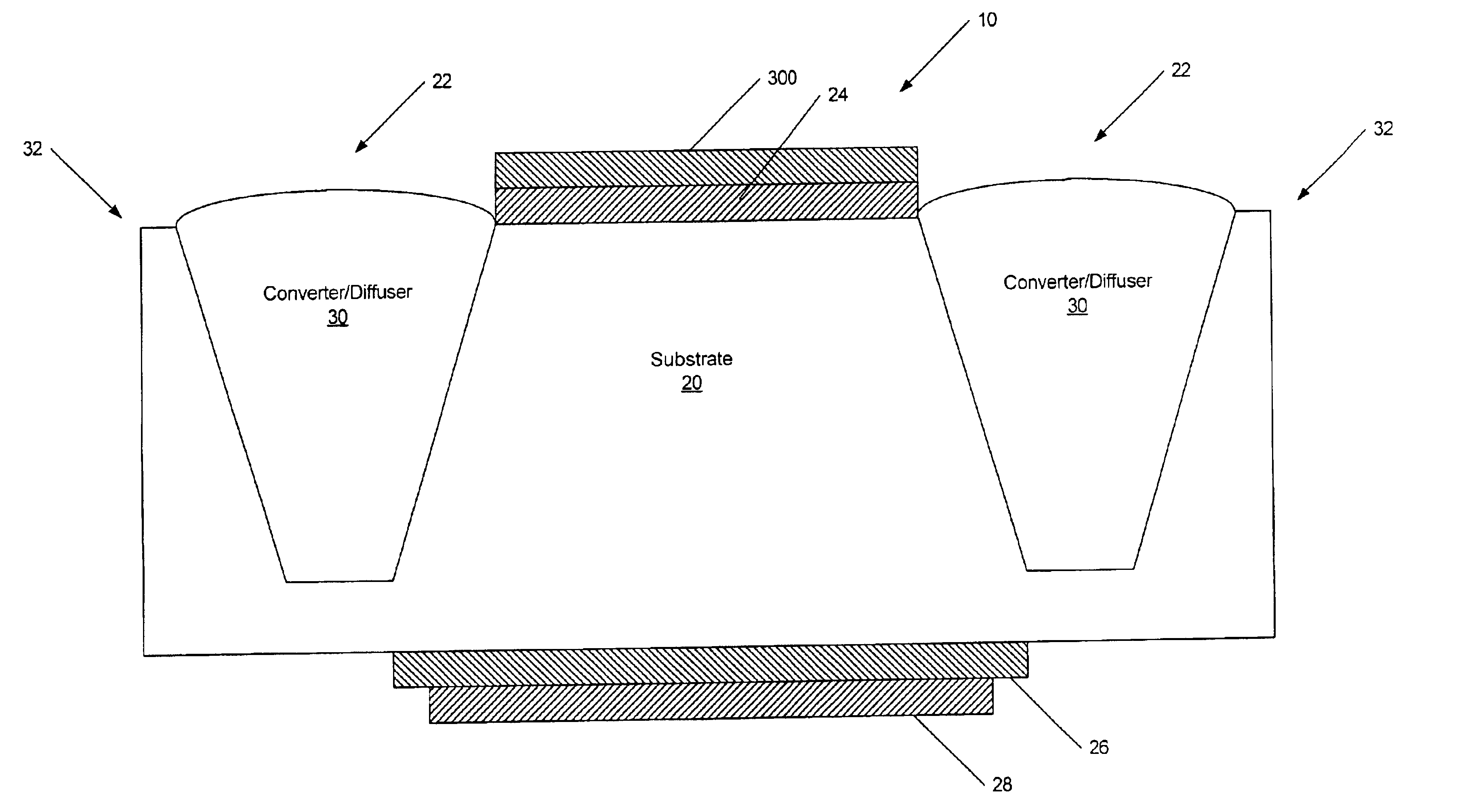
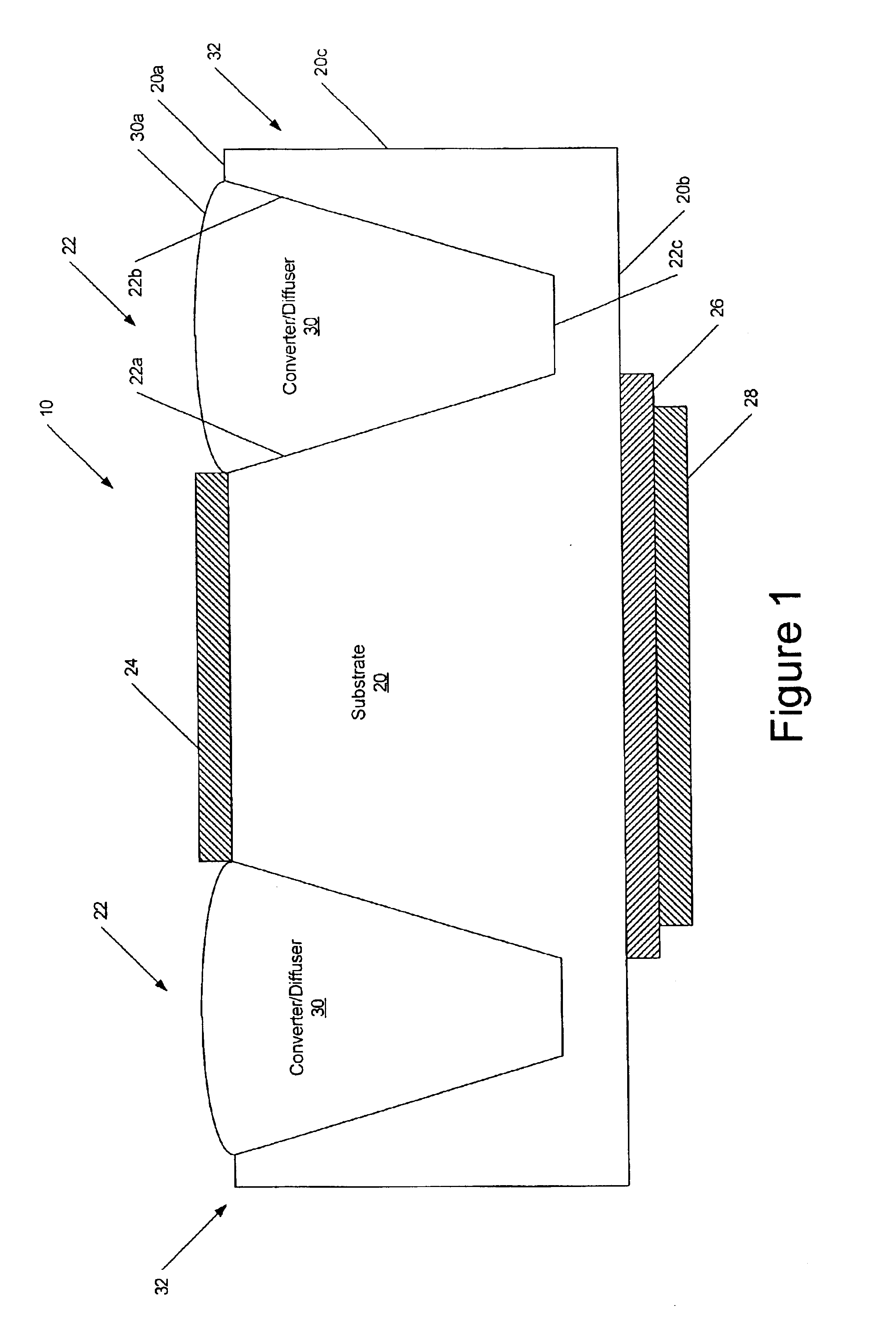
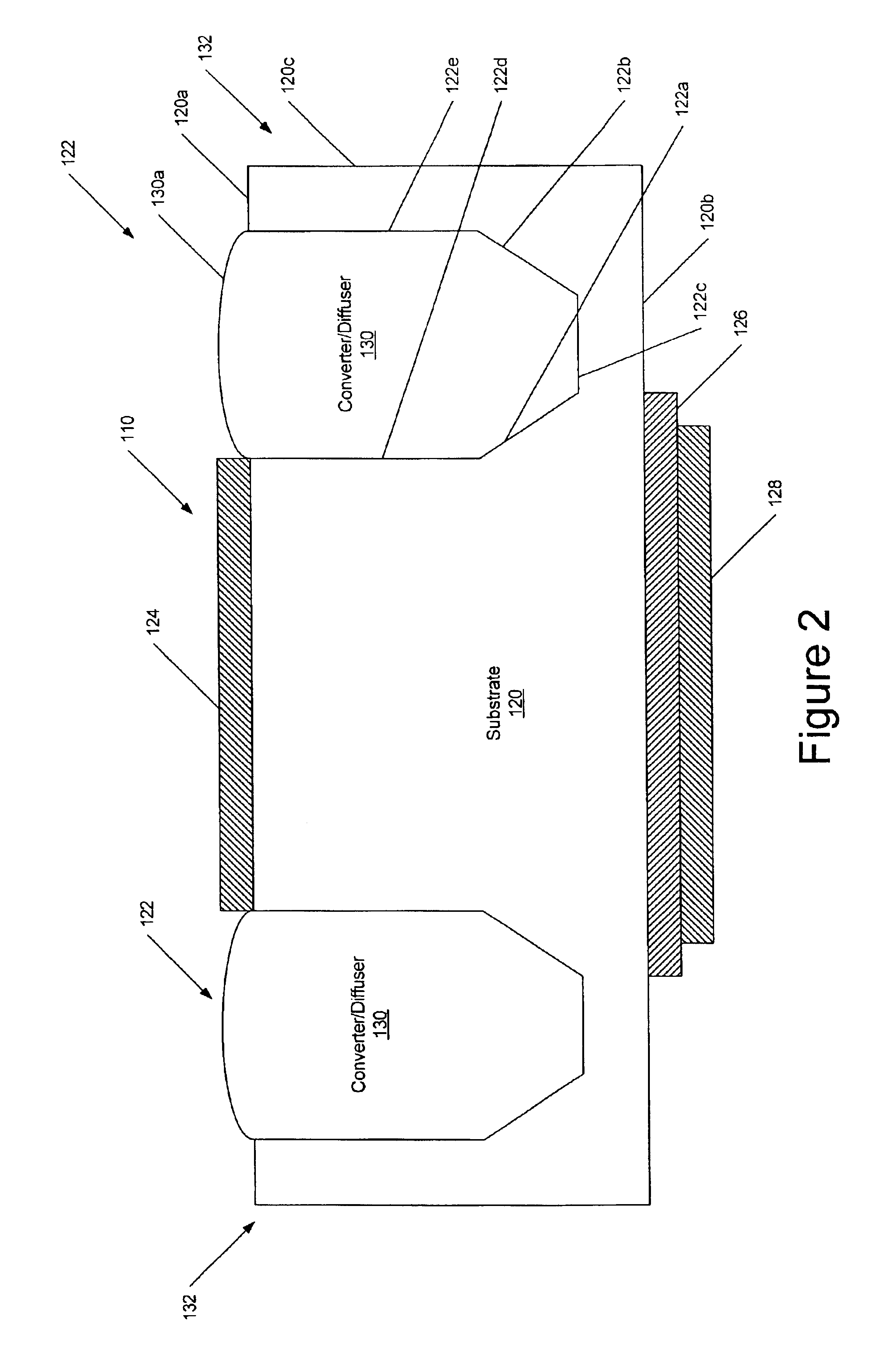
[0027]The present invention now will be described more fully hereinafter with reference to the accompanying drawings, in which embodiments of the invention are shown. This invention, however, should not be construed as limited to the embodiments set forth herein. Rather, these embodiments are provided so that this disclosure will be thorough and complete, and will fully convey the scope of the invention to those skilled in the art. In the drawings, the thickness of layers and regions are exaggerated for clarity. It will be understood that when an element such as a layer, region or substrate is referred to as being “on” or extending “onto” another element, it can be directly on or extend directly onto the other element or intervening elements may also be present. In contrast, when an element is referred to as being “directly on” or extending “directly onto” another element, there are no intervening elements present.

[0028]FIG. 1 illustrates certain embodiments of the present invention...


PUM


Abstract

Broad spectrum light emitting devices and methods and semiconductor chips for fabricating such devices include a light emitting element, such as a diode or laser, which emits light in a predefined range of frequencies. The light emitting element includes a shaped substrate suitable for light extraction through the substrate and a cavity in the substrate proximate the light emitting element. For example, a trench adjacent at least a portion of the periphery of the light emitting element may be provided. The cavity / trench is configured to contain light conversion material such that light extracted from sidewalls of the cavity / trench passes through the light conversion material contained in the cavity / trench. Methods of fabricating such devices and / or chips are also provided.

Description

FIELD OF THE INVENTION[0001]The present invention relates to semiconductor devices, and more particularly to semiconductor devices for producing light.BACKGROUND OF THE INVENTION[0002]Broad spectrum light emitting semiconductor devices have conventionally been fabricated by exciting a luminous substance with a relatively narrow spectrum light source. Conventionally, in such devices a light emitting diode (LED) or laser emits light in a narrow spectrum that is shifted and / or spread (i.e. converted) to provide a broader spectrum of light or a device with an output spectrum shifted from one range of the spectrum to another (e.g. blue to yellow, blue to green or to blue-green, or the like). Typically, it is desirable to provide white light from a narrow spectrum light source, such as an LED or laser. Such white light sources are described, for example, in U.S. Pat. No. 6,245,259, the disclosure of which is incorporated herein by reference as if set forth fully herein.[0003]Conventional ...

Claims


Application Information

Patent Timeline
26 Apr 2005
Publication
US6885033B2
IPC
H01L33/00; H01L33/20; H01L33/50
CPC
H01L33/508; H01L33/20
Inventors
ANDREWS, PETER S.