Nonvolatile semiconductor memory device

a semiconductor memory and non-volatile technology, applied in static storage, digital storage, instruments, etc., can solve the problems of inability to distinguish between written state and erased state, increase the threshold value of a cell in erased state gradually, and adversely influence the charge retention characteristi

Inactive Publication Date: 2005-05-17
KIOXIA CORP
View PDF11 Cites 140 Cited by
  • Summary
  • Abstract
  • Description
  • Claims
  • Application Information

AI Technical Summary

Problems solved by technology

However, this method has the following problem.
This might make it impossible to distinguish between the written state and the erased state.
A similar problem arises in a case where the threshold value of a cell in the erased state increases gradually to the extent that it cannot be distinguished from the written state.
The increase in the amount of charge in the charge storage electrode makes it easier for the charge to escape from the charge storage electrode through its electric field, which adversely influences the charge retention characteristic.
Therefore, in the prior art, it is difficult to make the increase of the number of program and erase cycles compatible with the securing of a sufficient threshold margin for data collapse.
However, even if the initial threshold voltage and the write speed are independent factors, the same reasoning holds because the condition of FIG. 3 is the worst one that will probably happen.
This results in an increase in the write time.
As a result, the stress electric field causes a dielectric breakdown of the tunnel insulating film or an increase in the interface level or in the fixed charge traps, which result in the deterioration of the charge retention characteristic and a shift in the threshold voltage after writing and erasing are done repeatedly.
This causes a reliability problem.
That is, when making ΔVpgm larger increases ΔVth, it is necessary to raise Vread, which decreases the reliability of the memory cells.
Moreover, in cells written into too high threshold voltage, the number of charges passing through their gate electrode film is large, which causes the problem of degrading the gate insulating film due to repetitive rewrite operations.
For the above reasons, it is difficult to make a high-speed write operation compatible with high reliability (a narrow threshold width).
In this method, however, either the high-speed write operation or the narrow threshold distribution is given priority by mode selection, but both of them cannot be satisfied at the same time.
As described above, with the conventional MONOS cell, it is difficult to make the increase in the number of repeatable rewrite operations compatible with securing a threshold margin for data collapse.

Method used


Image

  • Nonvolatile semiconductor memory device
  • Nonvolatile semiconductor memory device
  • Nonvolatile semiconductor memory device

Examples


first embodiment

[0119][First Embodiment]

[0120]A MONOS flash memory according to a first embodiment of the present invention will be explained. In a MONOS cell, if the captured charge centroid is in a place a distance of tox equivalent to oxide film thickness from the semiconductor substrate, the electric field in the tunnel oxide film is Eox, the capacitance between the captured charge centroid and the gate electrode is Cl, and the sum of the capacitance between the charge centroid and the control gate and the capacitance between the charge centroid and the semiconductor substrate is Ctot, these reference symbols can be considered in the same manner as those in a conventional floating-gate memory cell.

[0121]It is well known that writing data into a MONOS cell (that is, injecting electrons) can be expressed in FN tunnel current as into a floating-gate cell (reference 4: “Scaling of Multidieledtric Nonvolatile SONOS Memory Structures,” M. L. French and M. H. White, Solid State Electronics Vol. 37, No...

modification 1

[0149][Modification 1 of First Embodiment]

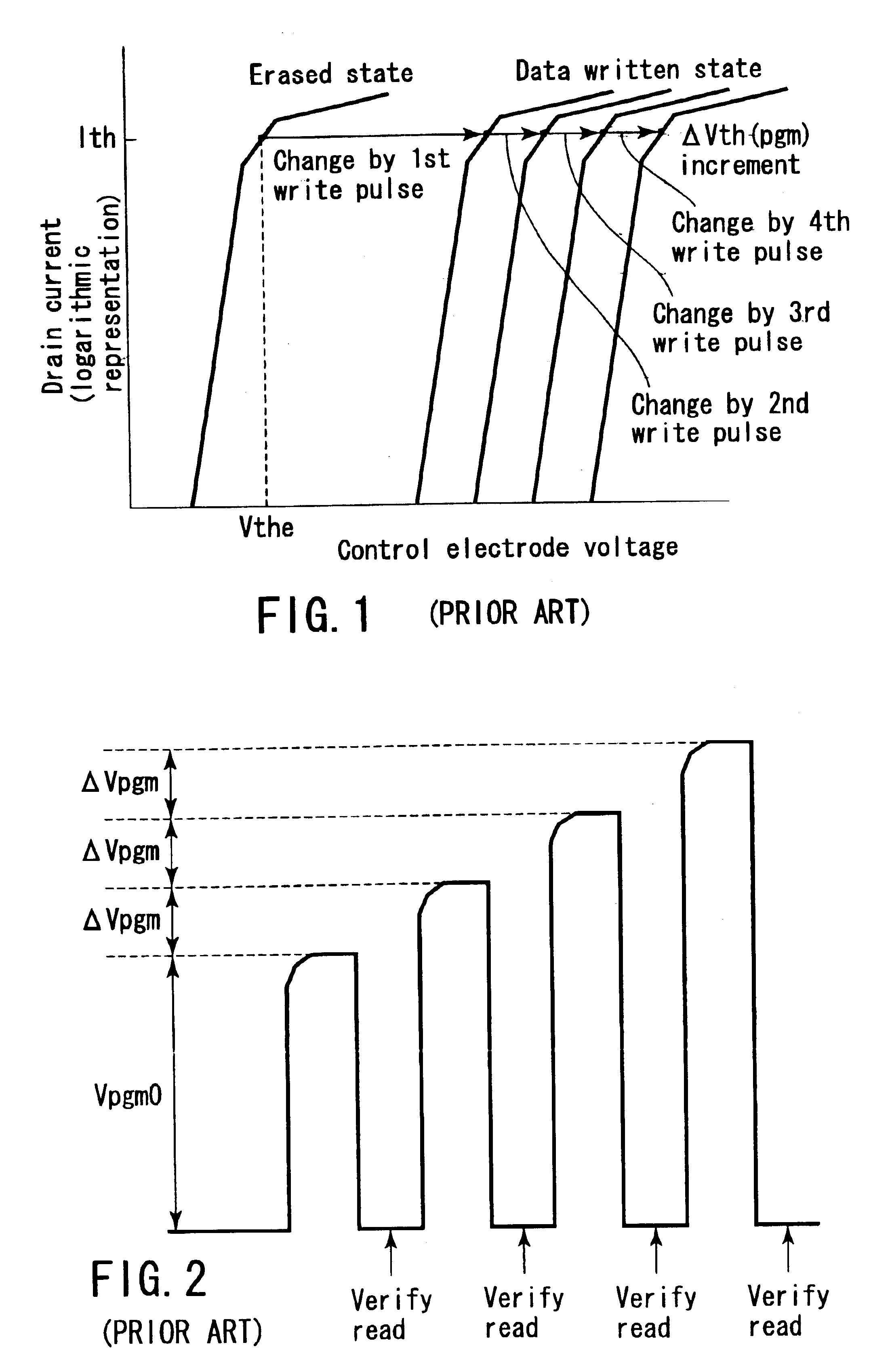
[0150]The case where a write pulse is applied only once in the first write operation has been explained. Next, a case where a pulse with a write start voltage of Vpgm0′ [V] is applied in the first write operation and thereafter a write operation is repeated a plurality of times (n>1) with a voltage raised in steps of the step-up voltage ΔVpgm1 will be explained.

[0151]FIGS. 10 and 11 correspond to FIGS. 6 and 8, respectively. A broken line in FIG. 11 shows the case of the comparative example (ΔVth(pgm1)=ΔVth(pgm2)).

[0152]As shown in FIG. 10, in modification 1, two write pulses are applied in the first write operation. During and after the first write operation, the thresholds voltages of all of the memory cells have not reached the write end decision voltage Vverify and therefore a verify operation is not needed. By doing this, the time required to make a write end verify determination can be reduced further. Here, when n>1, ΔVth(pgm1) is det...

second embodiment

[0187][Second Embodiment]

[0188]The effect of the first embodiment is not peculiar to the MONOS cell structure using an insulating film as a charge accumulation layer and is also expected even in a floating-gate cell structure with an ONO film intervening between a control gate electrode and a floating-gate electrode. The reason is that the ONO film has a stacked structure of a silicon oxide film, a silicon nitride film, and a silicon oxide film in that order and that the ONO film has the same stacked insulating film configuration as that of the stacked insulating film including the charge accumulation layer of a MONOS cell explained in the first embodiment.

[0189]When either the thickness of the upper oxide film of the ONO film or the thickness of the lower oxide film is decreased to 4 nm or less, an increase in the current flowing through the ONO film resulting from the injection of holes into the silicon nitride film is observed. This phenomenon has already been reported (reference...


PUM


Abstract

A cell array is configured by arranging a plurality of electrically writable erasable nonvolatile memory cells on a semiconductor substrate. Each of the memory cells has a charge accumulation layer formed via a first gate insulating film and a gate electrode formed on the charge accumulation layer via a second gate insulating film. A control circuit controls the sequence of writing and erasing the data into and from a memory cell selected in the memory cell. In writing the data into the memory cell, a first write operation is to apply a write pulse voltage with a first step-up voltage between the gate electrode and the semiconductor substrate. A second write operation is to apply a write pulse voltage with a second step-up voltage lower than the first step-up voltage.

Description

CROSS-REFERENCE TO RELATED APPLICATIONS[0001]This application is based upon and claims the benefit of priority from the prior Japanese Patent Applications No. 2002-179751, filed Jun. 20, 2002; and No. 2002-347798, filed Nov. 29, 2002, the entire contents of both of which are incorporated herein by reference.BACKGROUND OF THE INVENTION[0002]1. Field of the Invention[0003]This invention relates to a nonvolatile semiconductor memory device, and more particularly to a step-up write / erase operation.[0004]2. Description of the Related Art[0005]A floating-gate memory cell has been widely used as one of the electrically writable erasable nonvolatile semiconductor memory devices. A floating-gate memory cell has a structure where a floating gate and a control gate are stacked, on a semiconductor substrate. A tunnel oxide film of about 9 nm thick is formed between the semiconductor substrate and the floating gate. An ONO film equivalent to an oxide film of about 14 nm thick is formed between t...

Claims


Application Information

Patent Timeline
Patent Type & Authority Patents(United States)
IPC IPC(8): G11C16/34G11C16/04G11C16/06G11C16/00
CPCG11C16/3468G11C16/0466
Inventor YAEGASHI, TOSHITAKEGODA, AKIRANOGUCHI, MITSUHIRO
Owner KIOXIA CORP
Why Eureka
Try Eureka