Scannable synchronizer having a deceased resolving time

a synchronizer and dead technology, applied in the field of synchronizers, can solve the problems of limiting the speed of the master latch, and providing no gain to the signals, so as to reduce the resolving time associated with the master latch, reduce the possibility, and reduce the transition time of the input data signal

Inactive Publication Date: 2005-05-17
AVAGO TECH INT SALES PTE LTD
View PDF3 Cites 21 Cited by
  • Summary
  • Abstract
  • Description
  • Claims
  • Application Information

AI Technical Summary

Benefits of technology

[0017]Preferably, both the input stage and the transfer stage comprise a clocked inverter. The clocked inverter of the input stage provides gain to the input data signal that decreases the transition time of the input data signal and thereby decreases the possibility that the master latch will enter a meta-stable state, i.e., a state that the master latch must exit to begin driving the data signal to a 0 or a 1. The clocked inverter of the transfer stage provides gain to the signal being transferred from the master latch into the slave latch that decreases the possibility that the slave latch will enter a meta-stable state when the data signal output to the slave latch from the master latch has not already been resolved to a 0 or a 1 by the master latch.
[0018]The clocked inverter of the transfer stage also serves to isolate the master latch from the capacitance associated with the inverters of the slave latch during the portion of the clock cycle in which the master latch is attempting to resolve the data signal to a 0 or a 1. By isolating the master latch from this capacitance, the resolving time associated with the master latch is decreased.
[0019]These features of the present invention reduce the resolving time of the synchronizer and minimize the likelihood that a synchronizer failure will occur. These and other features and advantages of the present invention will become apparent from the following description, drawings and claims.

Problems solved by technology

One of the disadvantages associated with the synchronizer 1 is that when S1 goes high and M1 goes low, node MAS of the master latch 2 sees the capacitance associated with node SN2 of the slave latch 3.
Another disadvantage of the synchronizer 1 shown in FIG. 1 is that the input stage T1 of the master latch 2 and the input stage T4 of the slave latch 3 provide no gain to the signals being input to these latches.
Another disadvantage of the design of the synchronizer 1 shown in FIG. 1 is that, during testing of the synchronizer 1, both of the feedback inverters I1 and I3 of the master latch 2 must be overdriven by the transfer gate T2.
However, making gate T2 large increases the capacitance on node SN1 of the master latch 2, which, in turn, limits the speed with which the master latch 2 can resolve the data signal D to a 0 or a 1.

Method used


Image

  • Scannable synchronizer having a deceased resolving time
  • Scannable synchronizer having a deceased resolving time
  • Scannable synchronizer having a deceased resolving time

Examples


Embodiment Construction

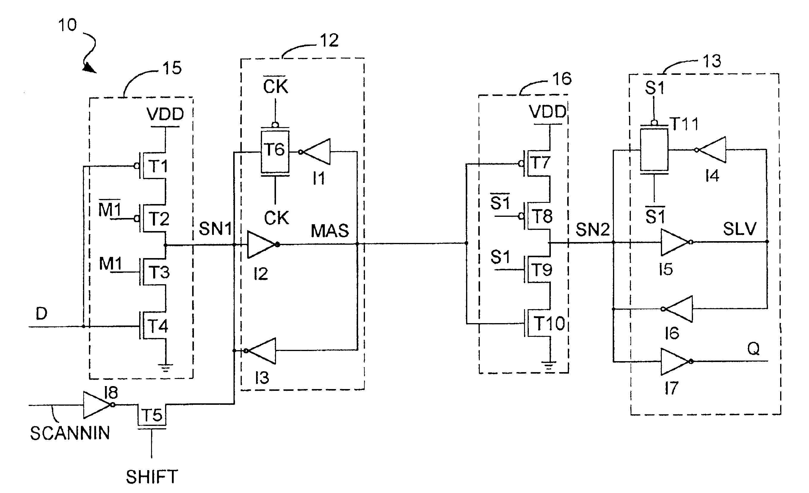
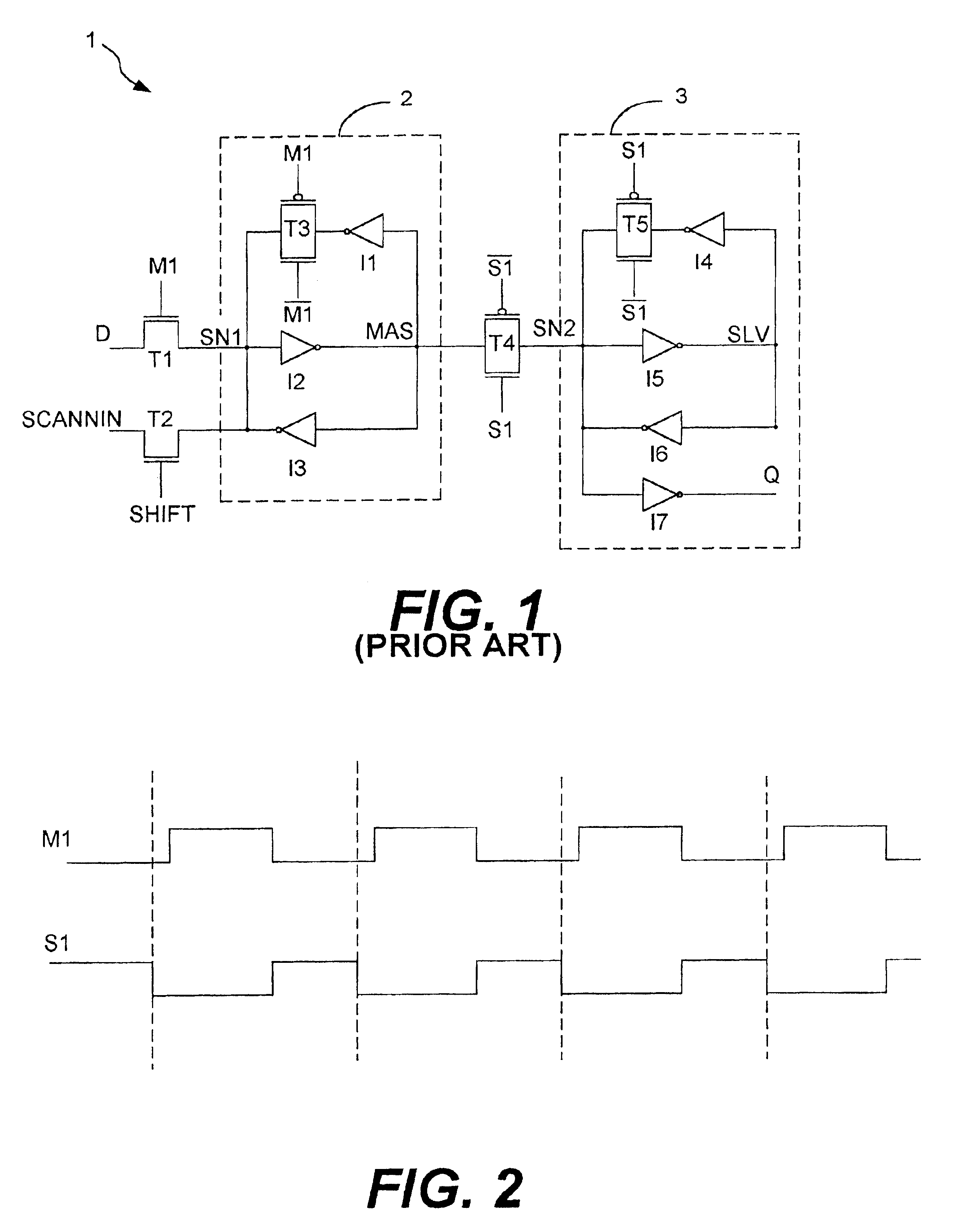
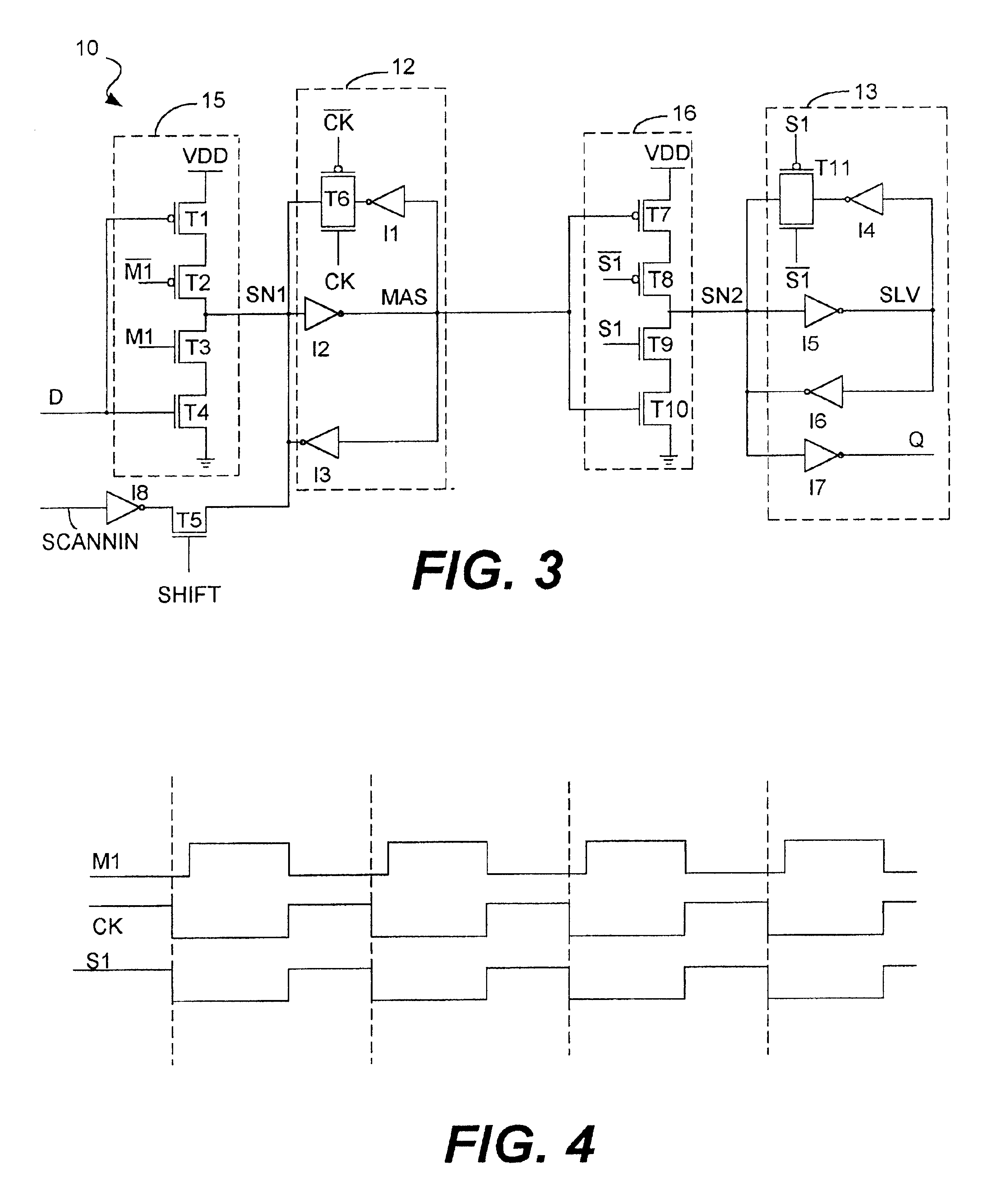
[0024]FIG. 3 is a schematic diagram of the synchronizer 10 of the present invention in accordance with the preferred embodiment. The synchronizer 10 comprises a master latch 12 and a slave latch 13. The master and slave latches 12 and 13 operate in a manner that is substantially identical to the manner in which the master and slave latches 2 and 3, respectively, shown in FIG. 1 operate. However, the synchronizer 10 of the present invention utilizes an input stage 15 to the master latch 12 and an input stage 16 to the slave latch 13 that are clocked inverters that facilitate the resolving processes performed by the master and slave latches 12 and 13, as described below in more detail. Therefore, the input stages 15 and 16 improve the resolving time of the synchronizer 10 and minimize the likelihood that a synchronizer failure will occur.

[0025]Another difference between the synchronizer 10 of the present invention and the synchronizer 1 shown in FIG. 1 is that the gate T6 is not contr...


PUM


Abstract

The present invention provides a synchronizer for receiving an incoming data signal of a first clock domain and for outputting a data signal of a second clock domain. The synchronizer comprises an input stage, a master latch, a transfer stage and a slave latch. The input stage receives the data signal of the first clock domain and outputs the data signal to the master latch when the input stage is clocked with a master clock signal. The master latch stores the data signal at a storage node of the master latch. The master latch has a resolve time associated with it during which the master latch seeks to resolve the data signal to a logic 0 or a logic 1. The transfer stage transfers the data signal stored in the master latch to the slave latch when the transfer stage is clocked with a slave clock signal.

Description

TECHNICAL FIELD OF THE INVENTION[0001]The present invention relates generally to synchronizers and, more particularly, to a scannable synchronizer having an improved design that enables the resolving time associated with the synchronizer to be decreased and that decreases the likelihood that a synchronizer failure will occur.BACKGROUND OF THE INVENTION[0002]Synchronizers receive data from upstream logic in one clock domain and synchronize that data to another clock domain associated with logic downstream of the synchronizer. The synchronizer ensures that the data coming out of the synchronizer will not violate the setup or hold constraints of clocked elements located downstream of the synchronizer. During synchronization, it is possible for the incoming data to violate the setup or hold constraints of the synchronizer itself, and thereby cause a meta-stable condition to occur in the synchronizer. The amount of time that it takes for the synchronizer to exit this meta-stable state an...

Claims


Application Information

Patent Timeline
Patent Type & Authority Patents(United States)
IPC IPC(8): H03K3/037H03K3/00
CPCH03K3/0372
Inventor STONG, GAYVIN E
Owner AVAGO TECH INT SALES PTE LTD
Why Eureka
Try Eureka