
Filtered connector

a technology of filtered connectors and connectors, applied in the direction of coupling device connections, coupling device details, printed circuit non-printed electric components association, etc., can solve the problems of additional labor and parts, considerable hand labor, etc., and achieve the effect of low cost and convenient soldering to the pin

Inactive Publication Date: 2005-05-24
ITT MFG ENTERPRISES LLC
View PDF5 Cites 18 Cited by
  • Summary
  • Abstract
  • Description
  • Claims
  • Application Information

AI Technical Summary

Benefits of technology

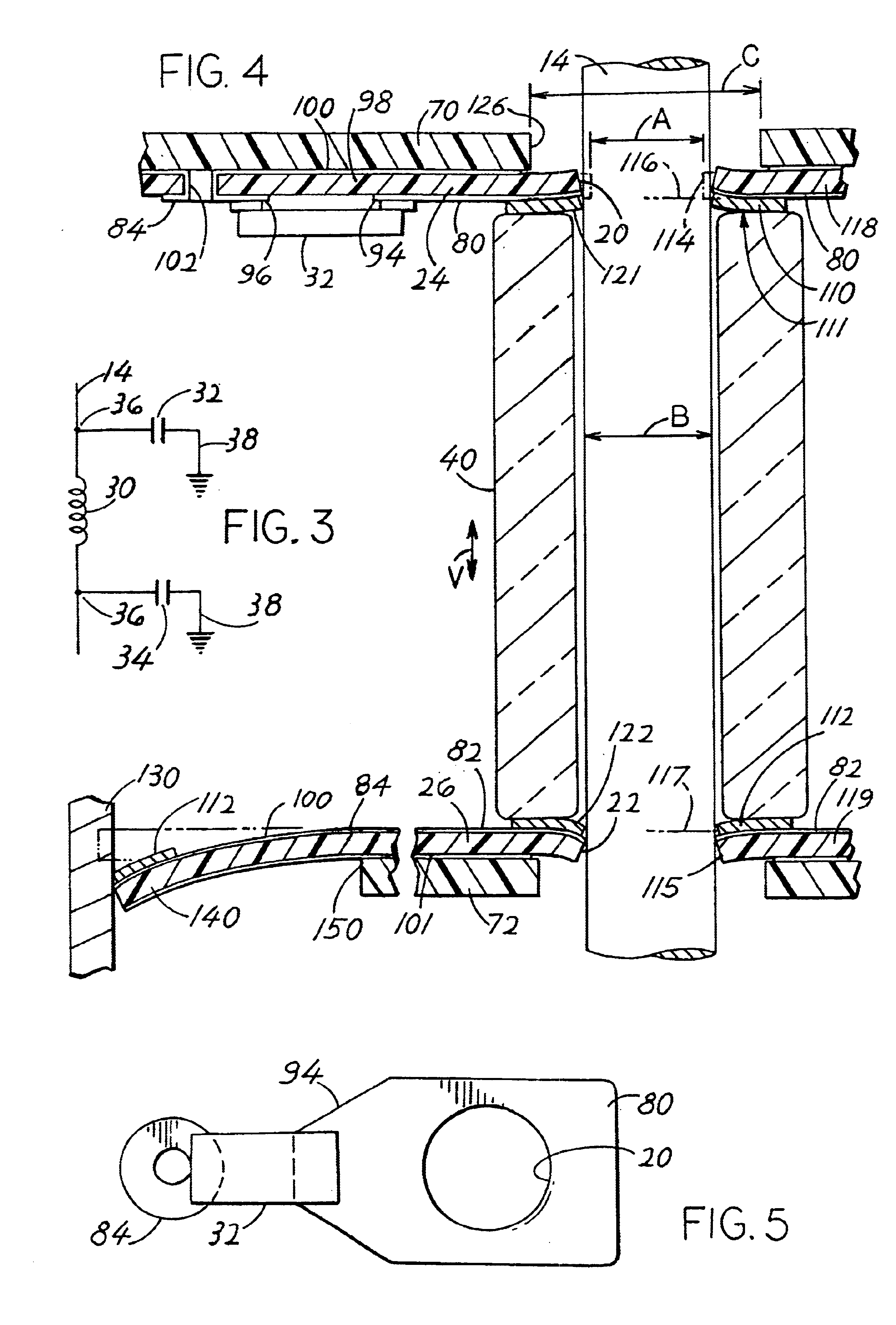
[0002]In accordance with one embodiment of the present invention, a filtered connector is provided, of the type that has a pair of spaced parallel circuit board portions with aligned holes that receive pin contacts, and that connect the pin contacts to filtering components, and a ground plane to a shell, which can be constructed at low cost. The two circuit board portions that lie in parallel planes, are parts of a single flexible circuit board which includes a loop portion that extends in a 180° loop to connect the board portions. Each board portion has signal traces that surround each hole and has ground traces, with filter components such as capacitors each soldered to a signal trace and to a ground trace. Each signal trace has walls at a pin-receiving hole, wherein the hole walls are bent out of the plane of the rest of the circuit board portion by the pin and are covered by a solder layer, to facilitate soldering to the pin. The periphery of at least one board portion is plated by a portion of a ground plane and is also deflected out of the plane of most of the board portion by the metal shell that surrounds the board portions and pins, and that is soldered to the shell.

Problems solved by technology

This has been accomplished by hand threading tiny solder rings around each pin until it lies against a signal trace, for vapor phase soldering, which involves considerable hand labor.
The ground planes of the two circuit boards can be connected together and to a metal shell by a separate deflectable contactor, but this involves additional labor and parts.

Method used


Image

  • Filtered connector
  • Filtered connector
  • Filtered connector

Examples


Embodiment Construction

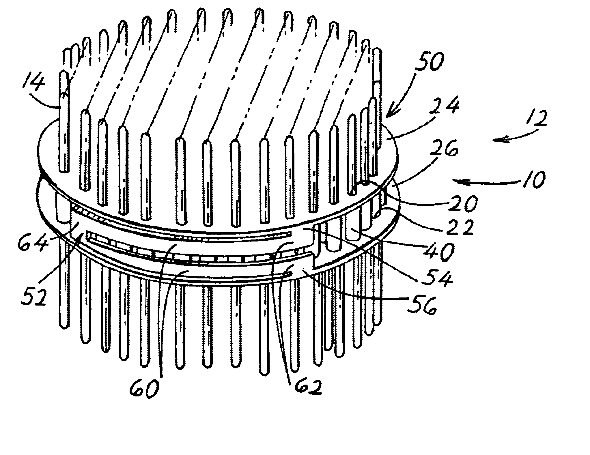
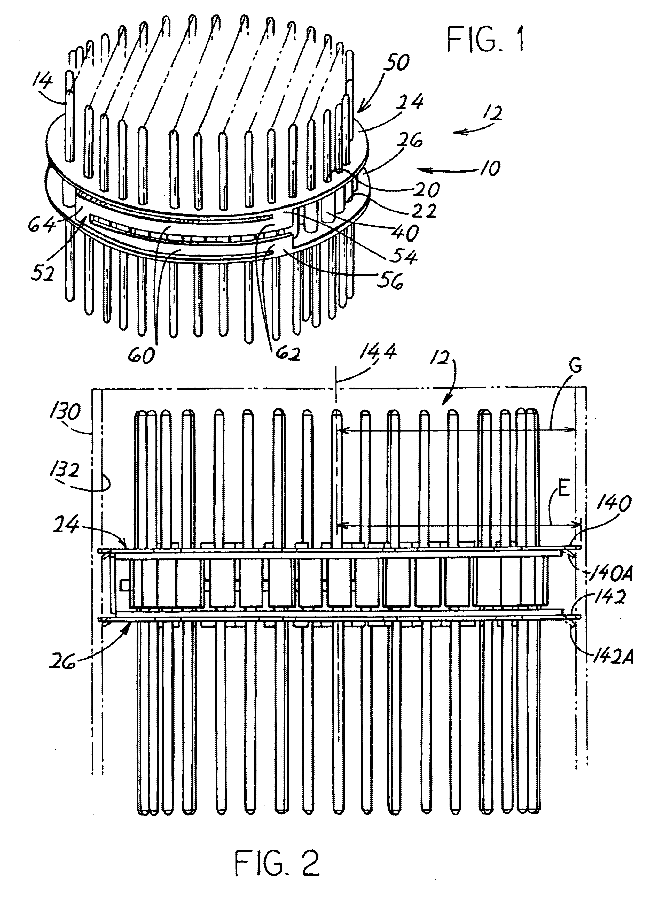
[0011]FIG. 1 illustrates a major portion 10 of a filtered connector 12, which includes numerous rows of pin contacts 14. By “pin contacts” applicant means that the contact has at least one end in the form of a male contact or pin. The pin contacts project through holes 20, 22 in each of two primarily flat circuit board portions, including a first or upper board portions 24 and a second or lower board portion 26. The connector is a filtered connector, wherein the connector provides a filter for each of the numerous pin contacts 14. Each filter is of the Pi type illustrated in FIG. 3, wherein an inductor 30 is coupled to the pin contact 14 and a pair of capacitors 32, 34 are also connected to the pin. Each capacitor has one end 36 connected to pin locations on opposite sides of the inductor, and each capacitor has an opposite end 38 that is grounded. FIG. 1 shows ferrite beads 40 that form the inductors.

[0012]In the prior art, the upper and lower flat board portions 24, 26 were each f...


PUM


Abstract

A filtered connector with multiple pin contacts (14) connected to ground by Pi filters, which can be constructed at low cost. Two circuit board portions (24, 26) that are spaced apart by ferrite beads (40), are portions of a single flexible circuit board (50) that are connected together by a loop portion (52) of the circuit board. A ground plane (100) of the circuit board is connected to a metal shell (130) that surrounds the circuit boards and pins, by bending peripheral portions (140, 142) of the circuit board as it is pressed into the shell and soldering the peripheral portions to the shell. Each of the pins is connected to a signal trace (80, 82) on the circuit board by the hole edge of each circuit board being deflected out of its original plane by the pin, to assure the flow of solder between the signal trace and the pin.

Description

BACKGROUND OF THE INVENTION[0001]One type of filtered connector includes a plurality of pin contacts that project through holes in circuit boards and through holes in ferrite beads that separate the circuit boards. One or more capacitors on each board provide the capacitors of a Pi filter for each contact. Signal traces on each board must be soldered to the pin contacts. This has been accomplished by hand threading tiny solder rings around each pin until it lies against a signal trace, for vapor phase soldering, which involves considerable hand labor. The ground planes of the two circuit boards can be connected together and to a metal shell by a separate deflectable contactor, but this involves additional labor and parts. A filtered connector of simple and low cost design, would be of value.SUMMARY OF THE INVENTION[0002]In accordance with one embodiment of the present invention, a filtered connector is provided, of the type that has a pair of spaced parallel circuit board portions w...

Claims


Application Information

Patent Timeline
IPC IPC(8): H01R13/719H05K1/18H01R13/66
CPCH01R13/7195H05K1/189
Inventor KOSMALA, MICHAEL LAWRENCE
Owner ITT MFG ENTERPRISES LLC
Learn More