Method for encapsulating organic electroluminescent device and an organic electroluminescent panel using the same

a technology of electroluminescent devices and organic materials, which is applied in the manufacture of electrode systems, cold cathode manufacturing, and electric discharge tubes/lamps, etc., can solve the problems of electroluminescent characteristics sharply degraded, second electrode formed on the organic layer may experience deterioration in performance, and the effect of increasing manufacturability

Inactive Publication Date: 2005-05-24
SAMSUNG DISPLAY CO LTD
View PDF7 Cites 45 Cited by
  • Summary
  • Abstract
  • Description
  • Claims
  • Application Information

AI Technical Summary

Benefits of technology

[0012]To solve the above-described problems, the present invention provides an encapsulating method of an organic EL device, which allows mass production, increases manufacturability and reduces a defect ratio, by effectively encapsulating the organic EL device against external moisture or oxygen.

Problems solved by technology

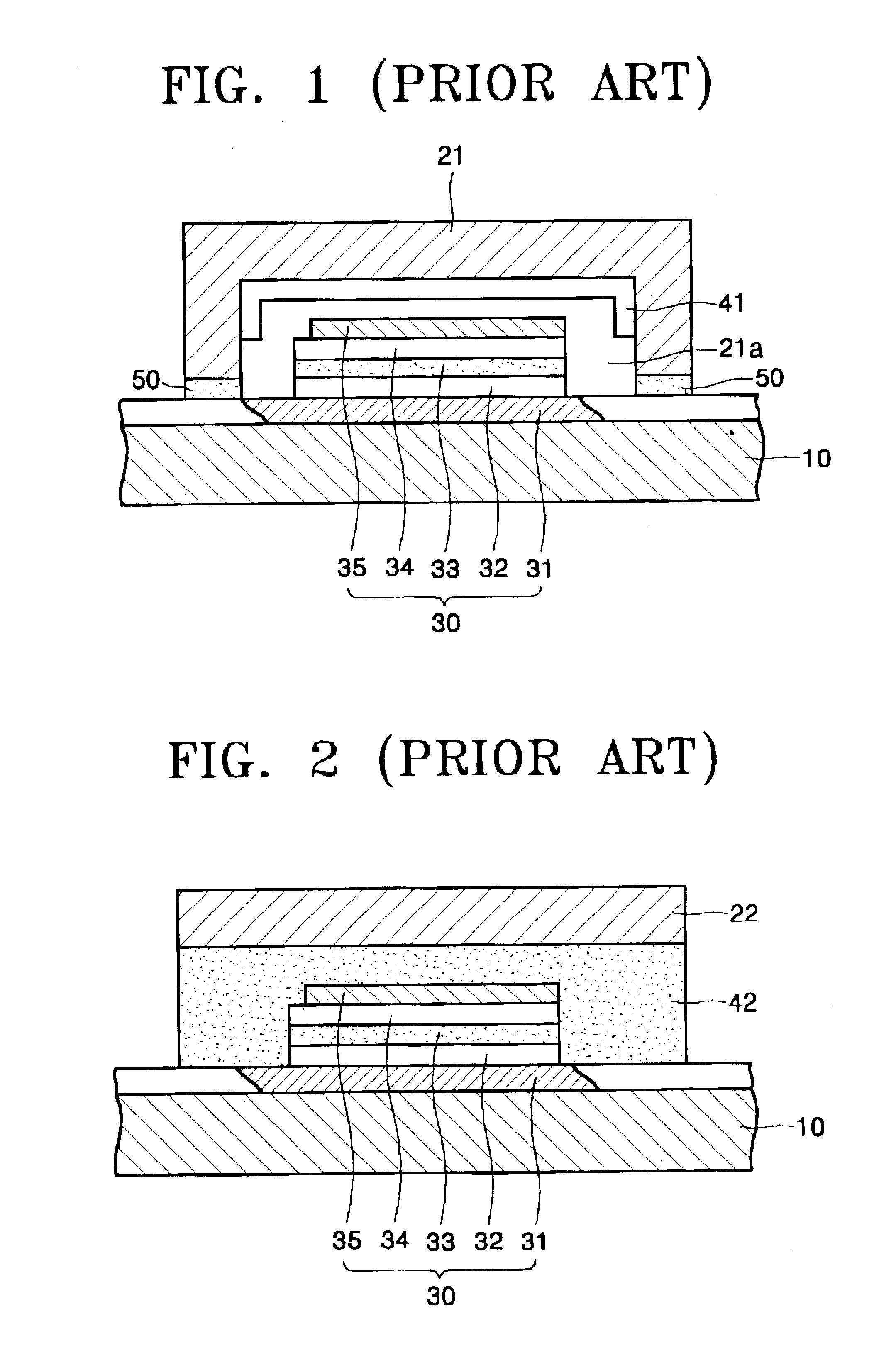
The organic layers made from organic compounds having low heat resistance are succeptible to deterioration due to moisture, and the second electrode formed on the organic layers may experience deterioration in performance.
As a result, when the organic EL device is driven in the presence of air, the electroluminescent characteristics sharply degrade.
This approach, however, involves several problems including an increase in cost, poor manufacturability and increased defect ratio.
This process results in poor manufacturability and increases the defect ratio for the product.
Another problem with this method is that the adhesion process may produce between the adhesive resin layer 42 and the encapsulation layer 22, and which, deteriorates the performance of the organic EL device 30.

Method used


Image

  • Method for encapsulating organic electroluminescent device and an organic electroluminescent panel using the same
  • Method for encapsulating organic electroluminescent device and an organic electroluminescent panel using the same
  • Method for encapsulating organic electroluminescent device and an organic electroluminescent panel using the same

Examples


example

[0034]An organic EL device was fabricated by sequentially depositing an anode formed of an ITO layer, a hole injection layer formed of IDE406, a hole transporting layer formed of IDE320, an emitting layer formed of CBP:lrppy, a hole blocking layer formed of Balq and a cathode layer formed of aluminum. An inert liquid layer was formed on the cathode layer.

[0035]The organic EL device was evaluated with and without a second sealant by measuring the growth of dark spots, i.e. the non-emmision area ratio, with the passage of time by microscopy. Measurements were taken at a brightness of 100 cd / m2. Table 1 shows the non-emmision area ratio measurements for 0 to 45 days for EL devices with and without a second sealant.

[0036]

TABLE 1Non Emission Area Ratio (%)TheWithoutAHSPassageSecond478XNR 5516DennumFluorinertof TimeSealantLV1HP8723LS-65EGC-1700Initial0.10.10.10.10.10.1 1 day0.10.10.10.10.10.1 5 days0.20.10.20.20.30.210 days0.50.10.30.30.50.220 days0.80.20.60.60.70.730 days1.10.31.00.90.91...


PUM


Abstract

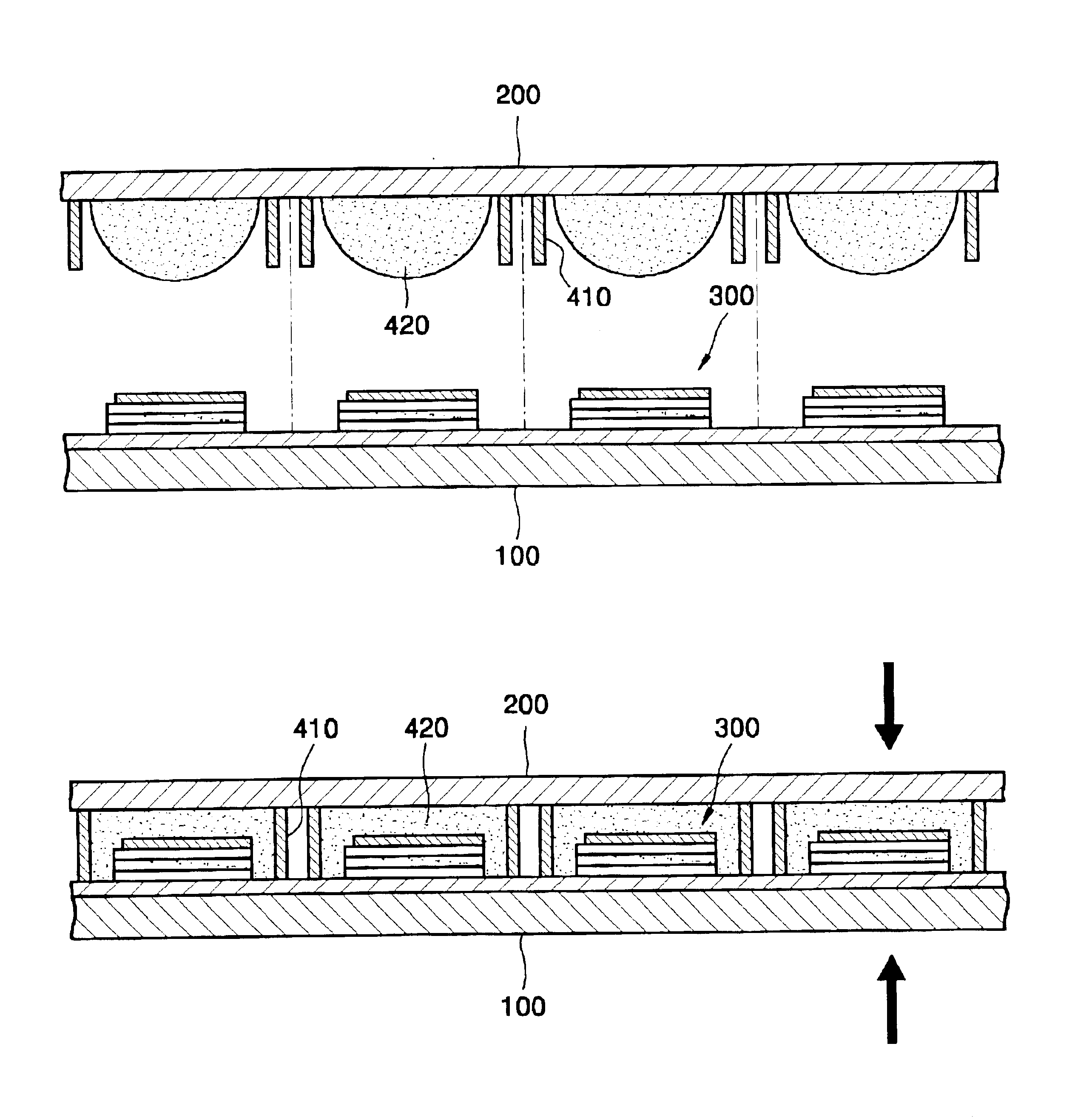
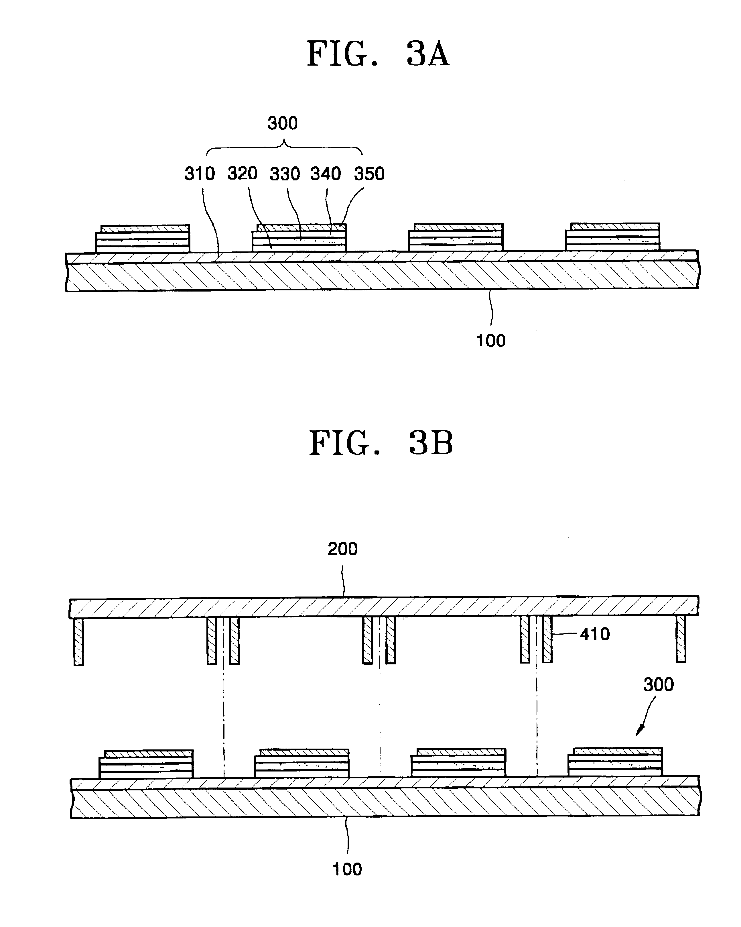
A method of encapsulating an organic electroluminescent (EL) device. The method includes applying a first sealant to a portion of an encapsulation plate facing a substrate to define one selected from a plurality of organic EL devices formed on the substrate, each including a first electrode layer, organic layers, and a second electrode layer. A space produced by the encapsulation plate and the first sealant and having an open face is filled with a second sealant. The substrate and the encapsulation plate are bonded together by applying pressure. The first sealant and the second sealant are then cured. The substrate and the encapsulation plate are cut into a plurality of independent organic EL panels.

Description

CROSS REFERENCE[0001]This application claims the benefit of Korean Patent Application No. 2002-0028714, filed on May 23, 2002, which is hereby incorporated by reference for all purposes as if fully set forth herein.BACKGROUND OF THE INVENTION[0002]1. Field of the Invention[0003]The present invention relates to an organic electroluminescent device, and more particularly, to an encapsulation method of an organic electroluminescent device by which the organic electroluminescent device is protected from moisture and oxygen infiltration, and an organic electroluminescent panel using the same.[0004]2. Description of the Related Art[0005]Recently, attention has been given to electroluminescent display devices as spontaneous emission display devices because they have advantageous features suitable for the next generation display devices, such as a wide viewing angle, a high contrast ratio and a high response speed. Electroluminescent display devices are classified into inorganic electrolumi...

Claims


Application Information

Patent Timeline
Patent Type & Authority Patents(United States)
IPC IPC(8): H01L51/52H01L51/56H01L51/50H05B33/04
CPCH01L51/5237H01L51/56H01L2251/566H10K71/851H10K71/00H10K59/873H10K59/8722H05B33/04H10K50/844H10K50/8426
Inventor PARK, JIN-WOOSONG, SEUNG-YONG
Owner SAMSUNG DISPLAY CO LTD
Why Eureka
Try Eureka