Fabrication of stacked microelectronic devices

a technology of microelectronic components and stacked components, which is applied in the direction of layered products, transportation and packaging, chemistry apparatus and processes, etc., can solve the problems of presenting manufacturing difficulties, limiting the density of the integrated circuit, and limiting the attachment of the second microelectronic component to the first microelectronic componen

Inactive Publication Date: 2005-05-24
MICRON TECH INC
View PDF47 Cites 52 Cited by
  • Summary
  • Abstract
  • Description
  • Claims
  • Application Information

AI Technical Summary

Problems solved by technology

Greater integrated circuit density is primarily limited by the space or “real estate” available for mounting microelectronic component on a substrate such as a printed circuit board.
If the first microelectronic component is electrically connected to the substrate by wire bonding, however, attachment of the second microelectronic component to the first microelectronic component can be more problematic.
The wires that electrically connect the active surface of the microelectronic component to the substrate accordingly interfere with attaching the second microelectronic component directly on the active surface.
However, a stacked microelectronic device such as that shown in FIG. 1 can present some manufacturing difficulties.
As the number of microelectronic components stacked atop one another in the microelectronic device increases, the chances for error increase concomitantly as one error in alignment or position of any layer of the stacked device can render the entire device unacceptable.

Method used


Image

  • Fabrication of stacked microelectronic devices
  • Fabrication of stacked microelectronic devices
  • Fabrication of stacked microelectronic devices

Examples


Embodiment Construction

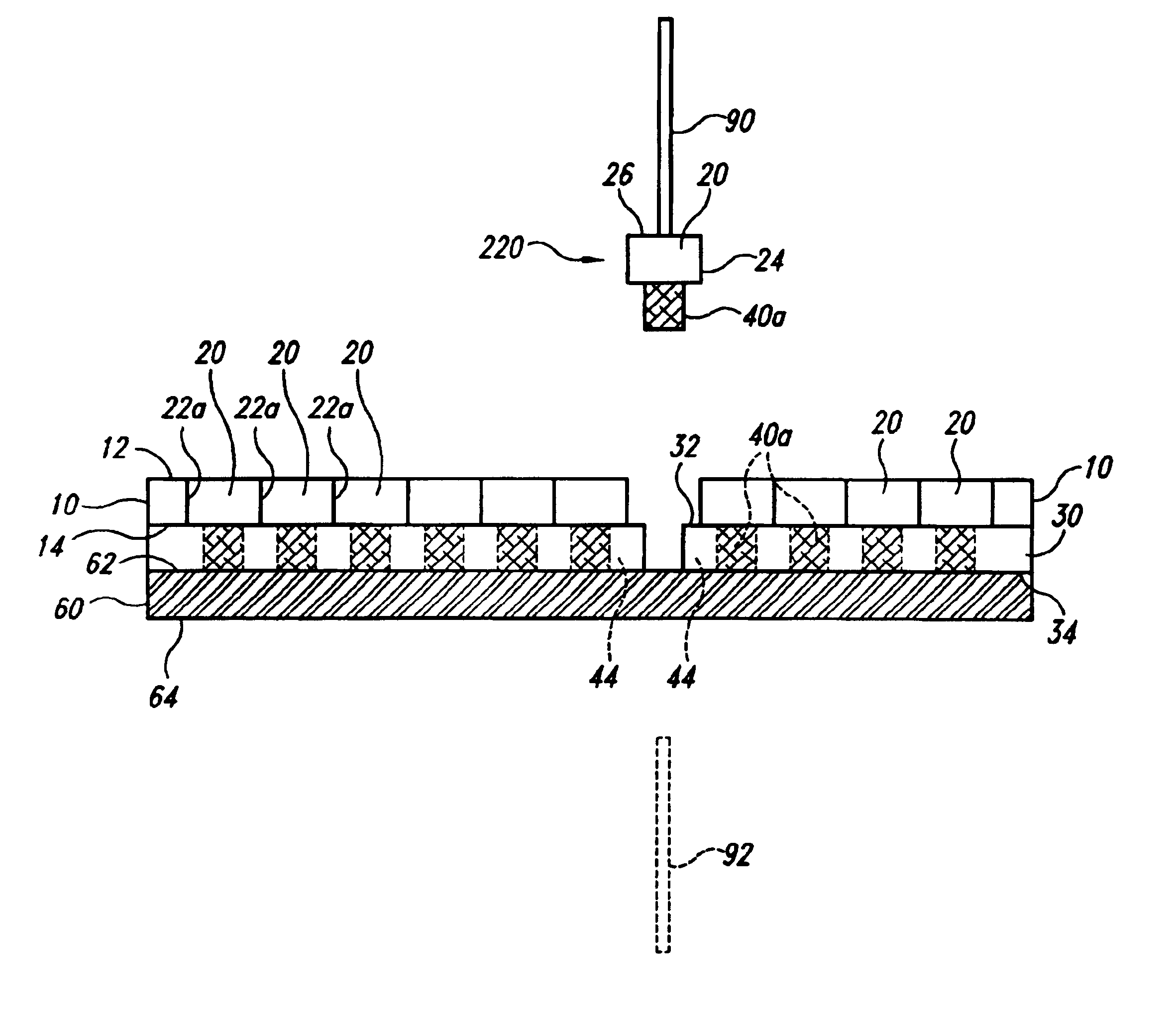
[0021]Various embodiments of the present invention provide methods of manufacturing stacked microelectronic devices and subassemblies useful in such manufacture. The following description provides specific details of certain embodiments of the invention illustrated in the drawings to provide a thorough understanding of those embodiments. It should be recognized, however, that the present invention can be reflected in additional embodiments and the invention may be practiced without some of the details in the following description.

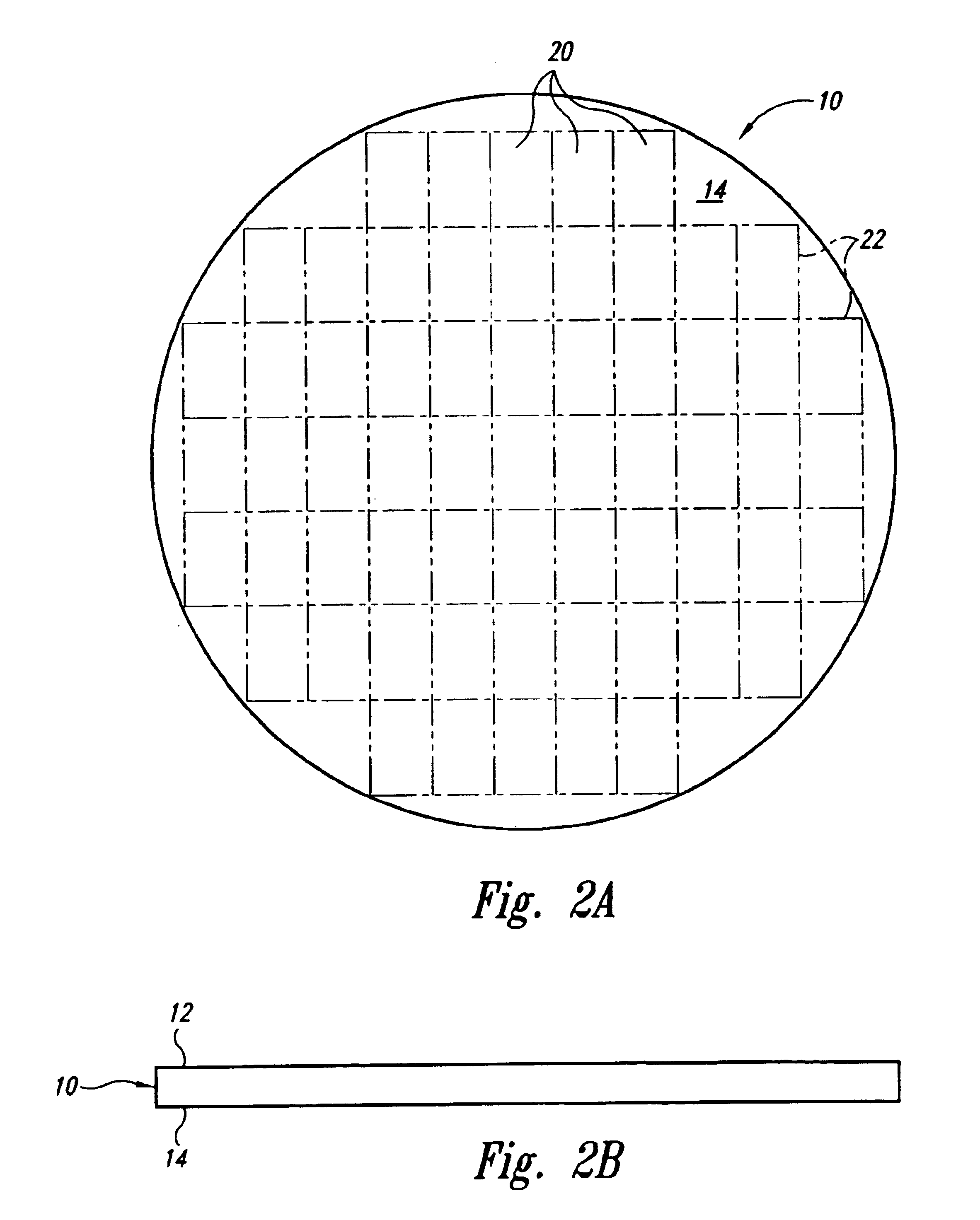
[0022]FIG. 2A illustrates a microelectronic wafer 10 having an active surface 12 and a rear surface 14. The wafer 10 may comprise a plurality of microelectronic components 20. For example, the wafer 10 may comprise a semiconductor wafer and each of the microelectronic components 20 may comprise a semiconductor die. Such semiconductor wafers are commonly manufactured as 200 mm or 300 mm discs with a plurality of semiconductor dies arranged in an array on the...


PUM

PropertyMeasurementUnit
thicknessaaaaaaaaaa
thicknessaaaaaaaaaa
adhesiveaaaaaaaaaa

Abstract

Manufacture of stacked microelectronic devices is facilitated by producing subassemblies wherein adhesive pads are applied to the back surfaces of a plurality of microelectronic components in a batch fashion. In one embodiment, an adhesive payer is applied on a rear surface of a wafer. A plurality of spaced-apart adhesive pads are defined within the adhesive layer. Each adhesive pad may cover less than the entire back surface area of the component to which it is attached. A mounting member (e.g., dicing tape) may be attached to the adhesive layer and, in some embodiments, the adhesive layer may be treated so that the mounting member is less adherent to the adhesive pads than to other parts of the adhesive layer, easing removal of the adhesive pads with the microelectronic components.

Description

TECHNICAL FIELD[0001]The present invention relates to methods and apparatus for increasing microelectronic component density. The invention has particular utility in connection with producing vertically superimposed, multi-component microelectronic devices in which at least one of the components is wire-bonded to a substrate.BACKGROUND[0002]Higher performance, lower cost, increased miniaturization of components, and greater packing density of integrated circuits are ongoing goals of the computer industry. Greater integrated circuit density is primarily limited by the space or “real estate” available for mounting microelectronic component on a substrate such as a printed circuit board. The microelectronic component may be electrically connected to circuitry on the circuit board via flip chip attachments, wire bonding, tape automated bonding (TAB), or a variety of other techniques.[0003]Increasingly, microelectronic components are being vertically stacked atop one another to conserve ...

Claims


Application Information

Patent Timeline
Patent Type & Authority Patents(United States)
IPC IPC(8): H01L21/70H01L21/98H01L21/58H01L21/68
CPCH01L21/6835H01L21/78H01L24/27H01L24/83H01L25/0657H01L25/50H01L21/6836H01L24/32H01L24/29Y10T428/1495H01L24/48H01L2221/68322H01L2221/68327H01L2224/274H01L2224/29007H01L2224/32014H01L2224/32145H01L2224/32225H01L2224/48091H01L2224/48227H01L2224/83191H01L2224/8385H01L2225/0651H01L2225/06575H01L2924/01005H01L2924/01013H01L2924/07802H01L2924/14Y10T156/1082H01L2924/01033Y10S438/976Y10T428/1457Y10T428/12535Y10T428/1443Y10T428/1471Y10T156/1092H01L2924/00014H01L2224/73265H01L2924/00H01L2224/45099H01L2224/45015H01L2924/207
Inventor CONNELL, MICHAELJIANG, TONGBI
Owner MICRON TECH INC
Why Eureka
Try Eureka