

Highly efficient OLEDs using doped ambipolar conductive molecular organic thin films
Inactive Publication Date: 2005-05-31
THE TRUSTEES FOR PRINCETON UNIV
View PDF32 Cites 34 Cited by
- Summary
- Abstract
- Description
- Claims
- Application Information
AI Technical Summary
Benefits of technology
[0011]The present invention is directed to simplified OLED structures comprising an anode layer, a hole injecting layer (HIL) in direct contact with the anode layer, an emissive electron transporting layer (ETL) in direct contact with the hole injecting layer, and a cathode layer in direct contact with the emissive electron transporting layer. The hole injecting material used in the hole injecting layer is c
Problems solved by technology
The remaining excitons in a fluorescent device, which are produced in the lowest triplet excited state of an organic molecule, are typically not capable of being converted into the en
Method used
View moreImage
Smart ImageViewing Examples

Examples
 PUM
| Property | Measurement | Unit |
|---|---|---|
| Ionization potential | aaaaa | aaaaa |
| Ionization potential | aaaaa | aaaaa |
| Electron affinity | aaaaa | aaaaa |
Abstract
The present invention is directed to simplified OLED structures comprising an anode layer, a hole injecting layer (HIL) in direct contact with the anode layer, an emissive organic electron transporting layer (ETL) in direct contact with the hole injecting layer, and a cathode layer in direct contact with the emissive organic electron transporting layer. The hole injecting material used in the hole injecting layer is characterized, in particular, as being an organic material having an ionization potential that is not more than about 0.7 eV greater than the ionization potential of the material used for the anode layer. The emissive organic electron transporting layer comprises an organic electron transporting material and an organic hole-trapping emissive material, for example, an organic phosphorescent material that produces emission from a triplet excited state of an organic molecule.
Description
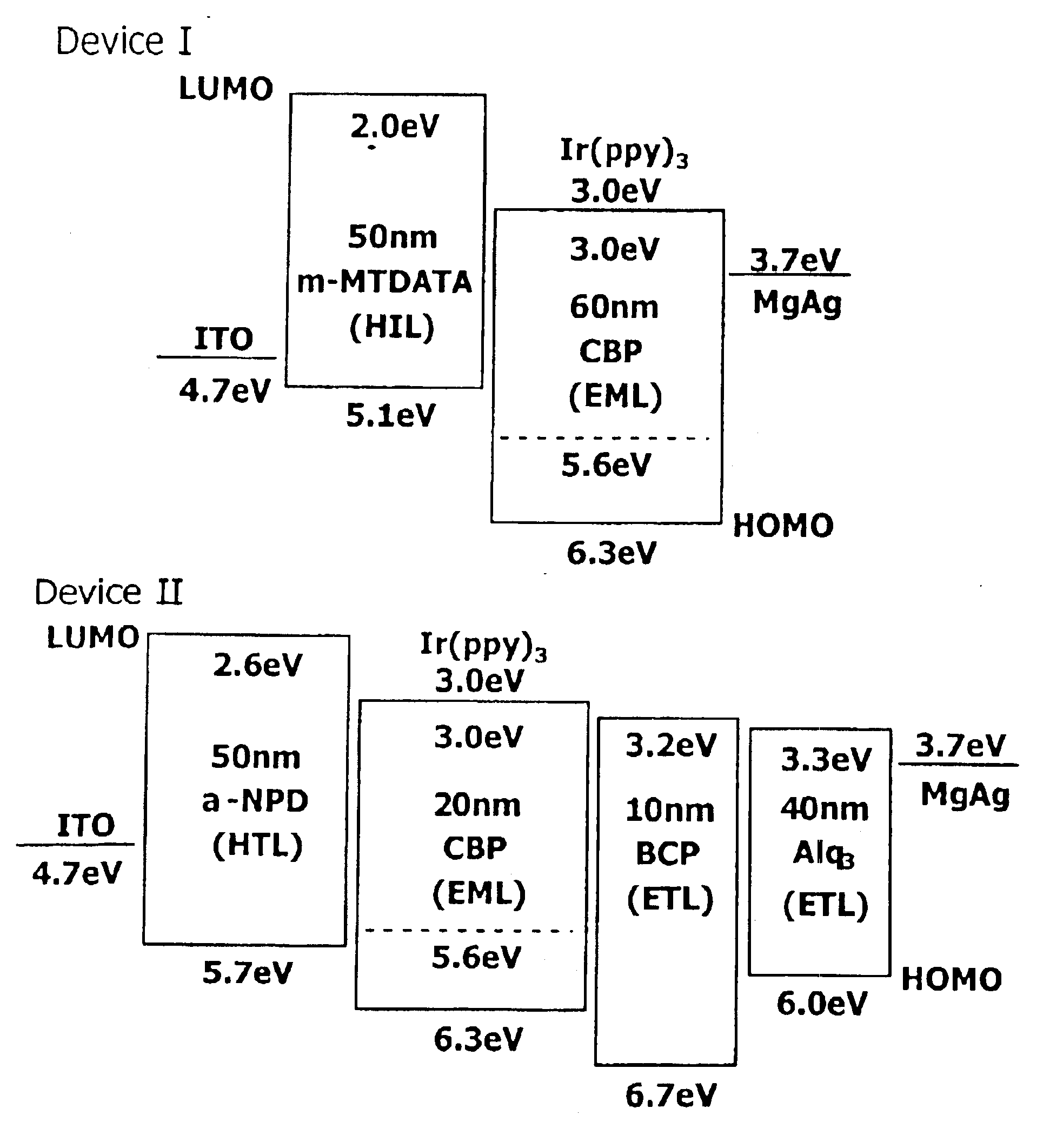
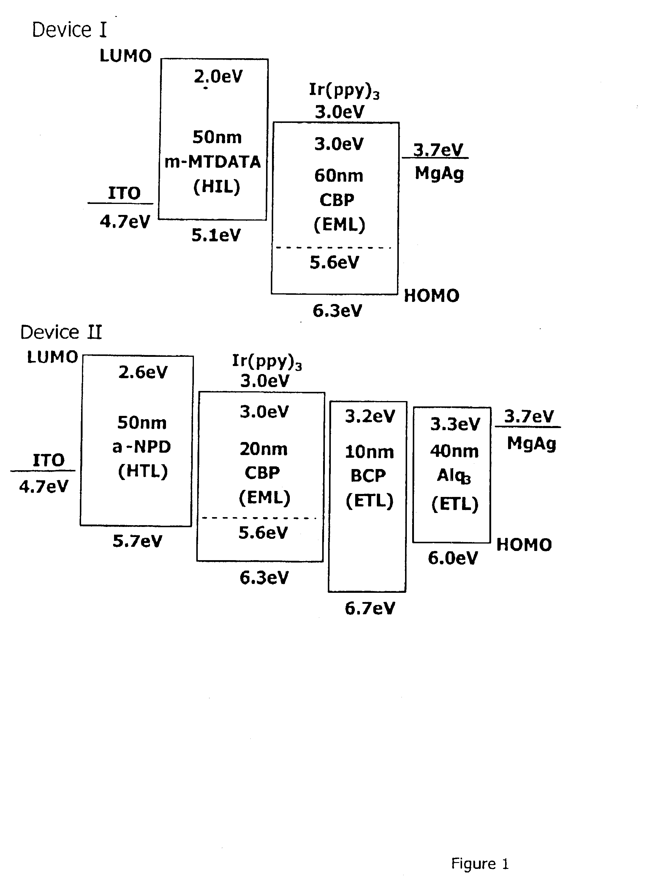
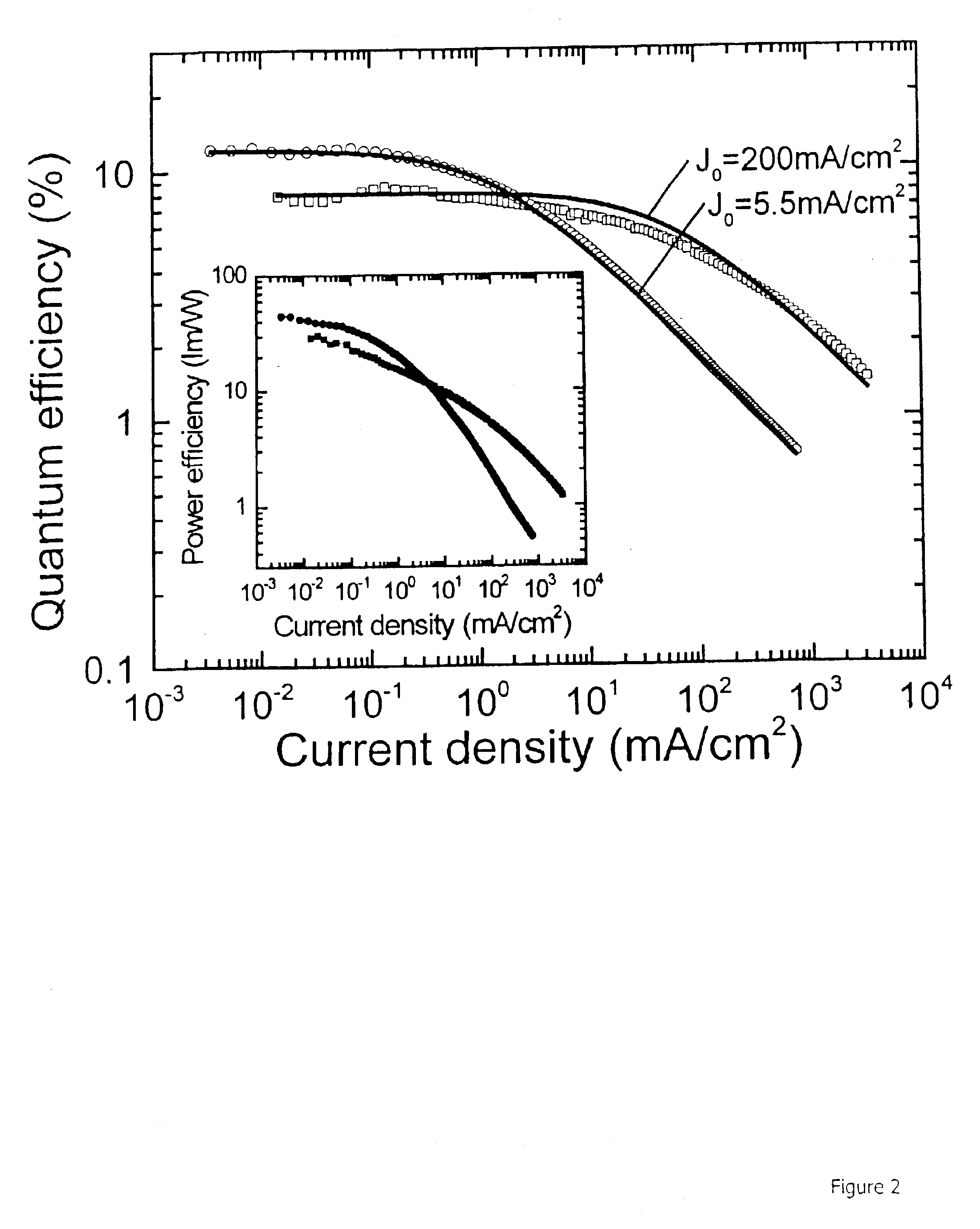
[0001]This application is a continuation of Ser. No. 09 / 740,183 filed Dec. 18, 2000 now U.S. Pat. No. 6,573,651.RESEARCH AGREEMENTS[0002]The claimed invention was made by, on behalf of, and / or in connection with one or more of the following parties to a joint university-corporation research agreement: Princeton University, The University of Southern California, and the Universal Display Corporation. The agreement was in effect on and before the date the claimed invention was made, and the claimed invention was made as a result of activities undertaken within the scope of the agreement.FIELD OF THE INVENTION[0003]The present invention relates to highly efficient organic light emitting devices (OLEDs) utilizing doped ambipolar conductive molecular organic thin films.BACKGROUND OF THE INVENTION[0004]Organic light emitting devices (OLEDs), which make use of thin film materials that emit light when excited by electric current, are expected to become an increasingly popular form of flat p...
Claims
Login to View More Application Information
Patent Timeline
 IPC IPC(8): H01L51/50H01L51/05H01L51/30H01L51/00
CPCH01L51/5088H01L51/5016H01L51/005H01L51/0059H01L51/0084Y10T428/24942H01L51/5048H10K85/60H10K85/631H10K85/341H10K50/11H10K2101/10H10K50/14H10K50/17
InventorADACHI, CHIHAYABALDO, MARC A.FORREST, STEPHEN R.
OwnerTHE TRUSTEES FOR PRINCETON UNIV