Organic el device

a technology of organic el and light source, which is applied in the direction of electroluminescent light source, chemistry apparatus and processes, and compositions of light source, can solve the problem of not being able to achieve high luminous efficiency of organic el devices, and achieve high luminous efficiency, high efficiency, and low cost

Active Publication Date: 2010-02-25
IDEMITSU KOSAN CO LTD
View PDF18 Cites 71 Cited by
  • Summary
  • Abstract
  • Description
  • Claims
  • Application Information

AI Technical Summary

Benefits of technology

[0038]Therefore, simply applying the typically-used host of fluorescent-emitting layer to the invention cannot satisfy the relationship represented by the above formula (1), nor provide an advantage of the invention that the triplet energy of the fluorescent-emitting layer is diffused to be used in emission of the phosphorescent dopant.
[0039]Unlike conventional ideas, the aspect of the invention adopts a material exhibiting a wide triplet energy gap as the host of the fluorescent-emitting layer, and realizes considerably highly-efficient emission with use of fluorescence and phosphorescence.
[0040]The triplet energy gap of the fluorescent host is preferably greater than 2.55 eV, more preferably 2.6 eV or more, further more preferably 2.7 eV or more.
[0041]When the triplet energy gap EgFH of the fluorescent host is wide, a range of material choices for the charge blocking layer that satisfies the above formula (1) can be expanded.
[0042]According to another known device, a singlet blocking layer for blocking the transfer of excited singlet energy is exemplarily provided between a phosphorescent-emitting layer and a fluorescent-emitting layer, so that mixed-color emission can be obtained at high efficiency by transferring only excited triplet energy of the fluorescent-emitting layer to the phosphorescent-emitting layer (e.g., the patent document 2).
[0043]However, simply providing the singlet blocking layer exhibiting a wide singlet energy gap does not lead to efficient transferring of the excited triplet energy from the fluorescent-emitting layer to the phosphorescent-emitting layer. Consequently, the luminous efficiency is not improved.

Problems solved by technology

As described above, organic EL devices capable of mixed-color emission at high luminous efficiency are not obtainable simply by layering blue fluorescent-emitting layers and red and green phosphorescent-emitting layers.

Method used


Image

  • Organic el device
  • Organic el device
  • Organic el device

Examples


first exemplary embodiment

[0201]The first exemplary embodiment of the invention will be shown in the drawings and described with reference to numerals allotted to components shown in the drawings.

(1) Arrangement of Organic EL Device

[0202]The followings are representative arrangement examples of the organic EL device:[0203](a) anode / emitting layer / cathode;[0204](b) anode / hole injecting layer / emitting layer / cathode;[0205](c) anode / emitting layer / electron injecting layer / cathode;[0206](d) anode / hole injecting layer / emitting layer / electron injecting layer / cathode;[0207](e) anode / organic semiconductor layer / emitting layer / cathode;[0208](f) anode / organic semiconductor layer / electron blocking layer / emitting layer / cathode;[0209](g) anode / organic semiconductor layer / emitting layer / adhesion improving layer / cathode;[0210](h) anode / hole injecting layer / hole transporting layer / emitting layer / electron injecting layer / cathode;[0211](i) anode / insulating layer / emitting layer / insulating layer / cathode;[0212](j) anode / inorganic...

second exemplary embodiment

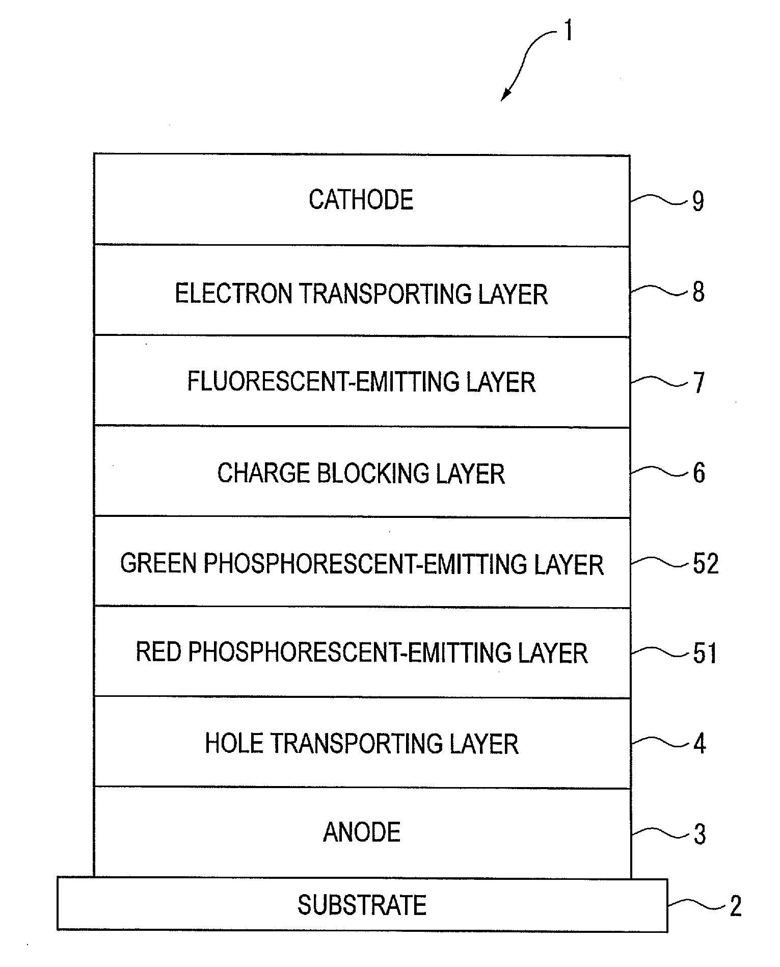
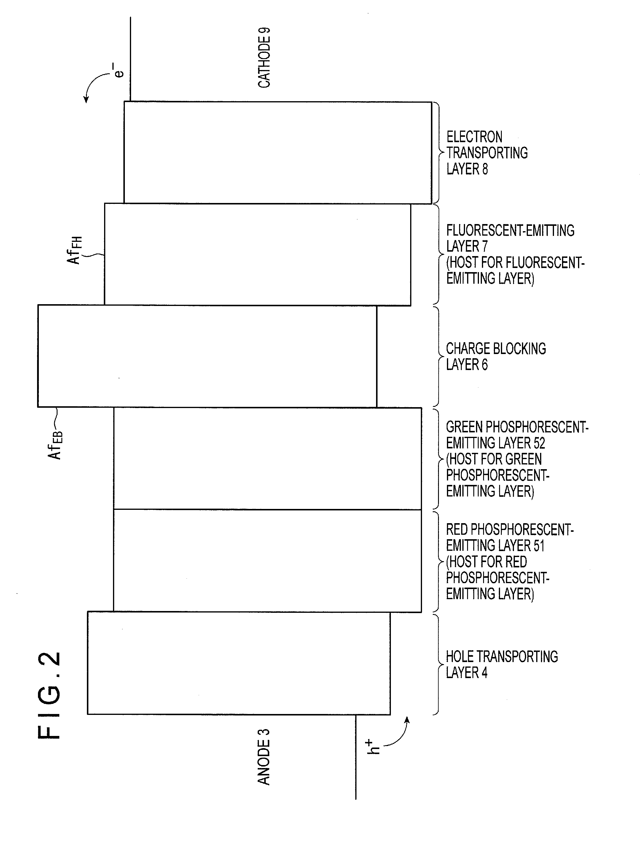
[0445]As shown in FIG. 4, an organic EL device of the second exemplary embodiment includes the anode 3, the hole transporting layer 4, the fluorescent-emitting layer 7, the charge blocking layer 6, the green phosphorescent-emitting layer 52, the red phosphorescent-emitting layer 51, the electron transporting layer 8 and the cathode 9, which are sequentially provided on the light-transmissive substrate 2.

[0446]Materials and manufacturing process are the same as in the first exemplary embodiment, but the the second exemplary embodiment is different from the first exemplary embodiment in the following points.

[0447]The charge blocking layer 6 blocks the holes injected into the fluorescent-emitting layer 7 from being injected toward the charge blocking layer 6 from the fluorescent-emitting layer 7, and injects the electrons from the phosphorescent-emitting layers 51 and 52 into the fluorescent-emitting layer 7.

[0448]Specifically, a triplet energy gap EgPD of the phosphorescent dopant, a ...

example 1

[0475]A glass substrate (size: 25 mm×75 mm×1.1 mm) having an ITO transparent electrode (manufactured by Geomatec Co., Ltd.) was ultrasonic-cleaned in isopropyl alcohol for five minutes, and then UV (Ultraviolet) / ozone-cleaned for 30 minutes.

[0476]After the glass substrate having the transparent electrode was cleaned, the glass substrate was mounted on a substrate holder of a vacuum deposition apparatus, and a hole transporting layer was initially formed by vapor-depositing 50-nm-thick TCTA(4,4′,4″-Tris(carbazol-9-yl)triphenylamine) to cover a surface of the glass substrate where a transparent electrode line was provided. The hole mobility of TCTA was 4×10⁻⁴ cm2 / Vs in an electric field of 10−4 to 10−6 V / cm.

[0477]A red phosphorescent-emitting layer was obtained by co-depositing CBP(4,4′-bis(N-carbazolyl)biphenyl) used as the red phosphorescent host and PQIr used as the red phosphorescent dopant onto the hole transporting layer to be 6 nm thick. The concentration of PQIr was 1 mass %.

[...


PUM

PropertyMeasurementUnit
thicknessaaaaaaaaaa
wavelengthaaaaaaaaaa
emission of a wavelengthaaaaaaaaaa

Abstract

A phosphorescent-emitting layer contains a phosphorescent host and a phosphorescent dopant for providing phosphorescence, and a fluorescent-emitting layer contains a fluorescent host and a fluorescent dopant for providing fluorescence. A charge blocking layer blocks electrons injected into the fluorescent host of the fluorescent-emitting layer from being injected toward the charge blocking layer from the fluorescent-emitting layer, and also injects holes into the fluorescent-emitting layer from the phosphorescent-emitting layer. A triplet energy gap EgPD of the phosphorescent dopant of the phosphorescent-emitting layer, a triplet energy gap EgEB of the charge blocking layer and a triplet energy gap EgFH of the fluorescent host of the fluorescent-emitting layer satisfy the following formula (1).EgPD<EgEB≦EgFH   (1)

Description

TECHNICAL FIELD[0001]The present invention relates to an organic EL device. In particular, the invention relates to an organic EL device including a plurality of emitting layers each of which emits different color light and from which mixed-color emission is obtainable.BACKGROUND ART[0002]To date, organic EL (electro-luminescence) devices including a plurality of emitting layers each of which emits light of a different wavelength are known. Such organic EL devices are also known to provide light of mixed color in which the light emitted by the emitting layers are mixed together. An example of such organic EL devices includes a red emitting layer, green emitting layer and blue emitting layer, and provides white-color light in which the light emitted by the emitting layers are mixed together.[0003]Excited state of organic compounds encompasses excited singlet state and excited triplet state. Emission obtained from excited singlet state is called fluorescence while emission obtained fr...

Claims


Application Information

Patent Timeline
Patent Type & Authority Applications(United States)
IPC IPC(8): H01L51/52
CPCC09K11/06C09K2211/1007C09K2211/1011C09K2211/1014H05B33/14H10K85/631H10K85/636H10K85/654H10K85/342H10K85/6572H10K50/131H10K50/11H10K2101/40H10K50/18H10K2101/10H10K2101/30
Inventor NISHIMURA, KAZUKIIWAKUMA, TOSHIHIROFUKUOKA, KENICHIJINDE, YUKITOSHIHOSOKAWA, CHISHIO
Owner IDEMITSU KOSAN CO LTD
Why Eureka
Try Eureka