Intermediate band semiconductor photovoltaic solar cell

a solar cell and semiconductor technology, applied in semiconductor devices, pv power plants, solid-state devices, etc., can solve the problems of inconvenient solar cells that do not completely convert the energy of the photons they receive into electric energy, and fail to use the excess energy provided by the photon

Inactive Publication Date: 2002-09-03
AUTONOMOUS UNIVERSITY OF MADRID +2
View PDF9 Cites 74 Cited by
  • Summary
  • Abstract
  • Description
  • Claims
  • Application Information

AI Technical Summary

Problems solved by technology

An inconvenience of the solar cells is that they do not completely convert the energy of the photons they receive into electric energy.
For photons with more energy, they also fail to the best use of the excess energy provided by the photon.

Method used


Image

  • Intermediate band semiconductor photovoltaic solar cell
  • Intermediate band semiconductor photovoltaic solar cell
  • Intermediate band semiconductor photovoltaic solar cell

Examples


Embodiment Construction

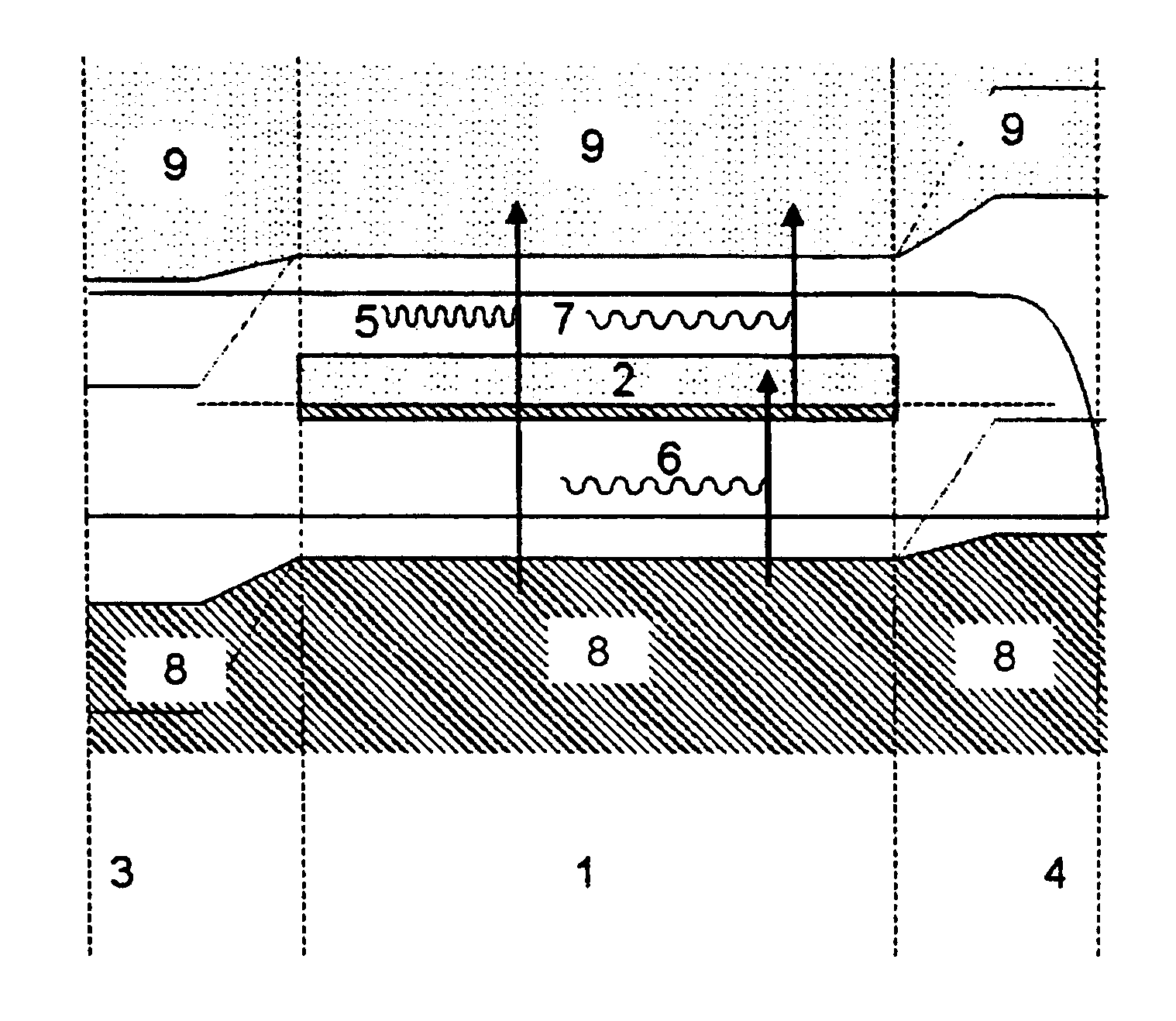
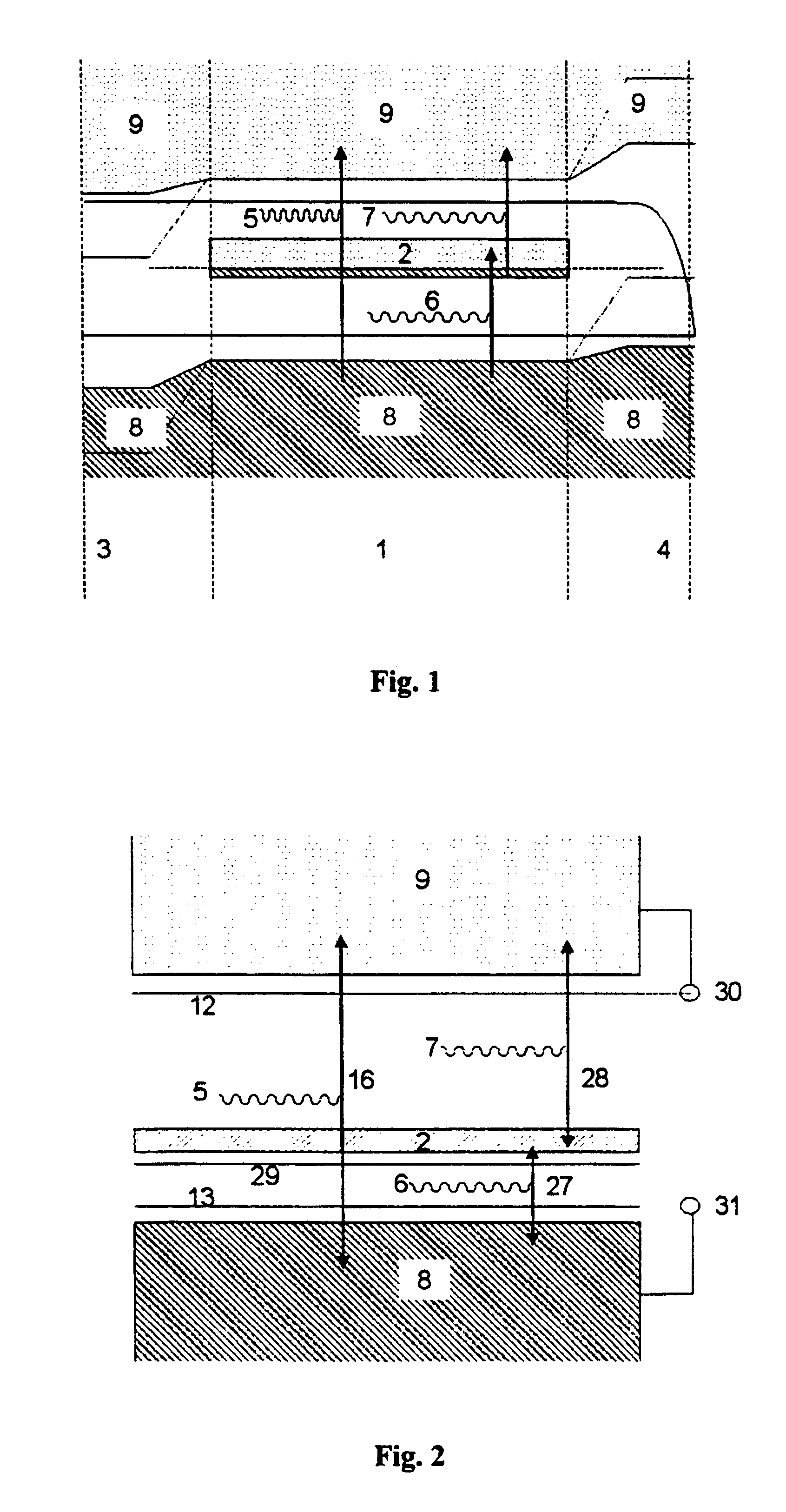
It is assumed that a semiconductor has an intermediate energy band like the one represented with (2) in FIG. 2. It also has, like the ordinary semiconductors, a conduction band (9) and a valence band (8). As in an ordinary semiconductor, the photons (5) can pump (16) electrons from the valence band (8) to the conduction band (9), creating electron-hole pairs. However, there are also photons (6) with less energy that pump (27) electrons from the valence band (8) to the intermediate band (2) and there are also other photons (7) that pump (28) electrons from the intermediate band to the conduction band (9). The concatenation of the pumping processes (27) of electrons from the valence band to the intermediate band and (28) from this to the conduction band complete the generation of an electron-hole pair.

Filling of the conduction n band (9) is caused as the difference between the pumping arising by means of the processes (16) and (28) and the drops through the same processes in the oppos...


PUM


Abstract

The invention relates to a solar cell containing a semiconductor (1) with an intermediate band (2) that is half filled with electrons, located between two layers of ordinary n type (3) and p type (4) semiconductors. When lighted, electron-hole pairs are formed either by a photon that absorbs the necessary energy (5) or by two photons (6,7) that absorb less energy which pump an electron from the valence band to the intermediate band (8) and from the latter to the conductance band (9). An electrical current is generated that exits on the p side and returns via the n side. The n and p layers also prevent the intermediate band from contacting the outer metal connections, which would have resulted in a short-circuit. Said cell converts solar energy into electricity in a more efficient manner than conventional cells and contributes to improvement of the photovoltaic devices.

Description

SUBJECTA solar cell able to convert solar energy into electricity is described, based on a new operative principle capable of obtaining efficiency superior to that obtained with the present solar cells. Therefore, this invention pertains to the scope of manufacturing semiconductor devices for electronic use and, more specifically, to the manufacture of solar cells.The cell, as described in FIG. 1, contains a semiconductor (1) with an intermediate band (2) half filled with electrons, located between two ordinary, n type (3) and p type (4), semiconductor layers. On lighting up electron-hole pairs are created, either by absorption of a photon with the required energy (5) or by the absorption of two (6,7) with less energy that pump an electron from the valence band to the intermediate band (8) and from this to the conduction band (9). A flow of electrons exits mainly through the n type (3) semiconductor and a flow of holes through the p type (4); thus an electric current that exits thro...

Claims


Application Information

Patent Timeline
Patent Type & Authority Patents(United States)
IPC IPC(8): H01L31/0352H01L31/0248H01L31/032H01L31/06
CPCH01L31/032H01L31/0352H01L31/06Y02E10/50
Inventor LUQUE-LOPEZ, ANTONIOFLORES-SINTA, FERNANDOMARTI-VEGA, ANTONIOCONESA-CEGARRA, JOSE CARLOSWAHNON-BENARROCH, PERLAORTEGA-MATEO, JOSETABLERO-CRESPO, CESARPEREZ-PEREZ, RUBENCUADRA-RODRIGUEZ, LUCAS
Owner AUTONOMOUS UNIVERSITY OF MADRID
Why Eureka
Try Eureka