Unipolar light emitting devices based on III-nitride semiconductor superlattices

a technology of iiinitride and semiconductor, applied in semiconductor devices, semiconductor lasers, semiconductor lasers, etc., can solve the problems of blocking the further development of high-power lasers and light-emitting diodes in the visible spectral rang

Inactive Publication Date: 2002-09-24
ARIMA OPTOELECTRONICS
View PDF14 Cites 79 Cited by
  • Summary
  • Abstract
  • Description
  • Claims
  • Application Information

AI Technical Summary

Problems solved by technology

However, there is a problem in getting a good p-type conductivity for these materials, which blocks further development of high power lasers and light emitting diodes for the visible spectral range.

Method used


Image

  • Unipolar light emitting devices based on III-nitride semiconductor superlattices
  • Unipolar light emitting devices based on III-nitride semiconductor superlattices
  • Unipolar light emitting devices based on III-nitride semiconductor superlattices

Examples


example 2

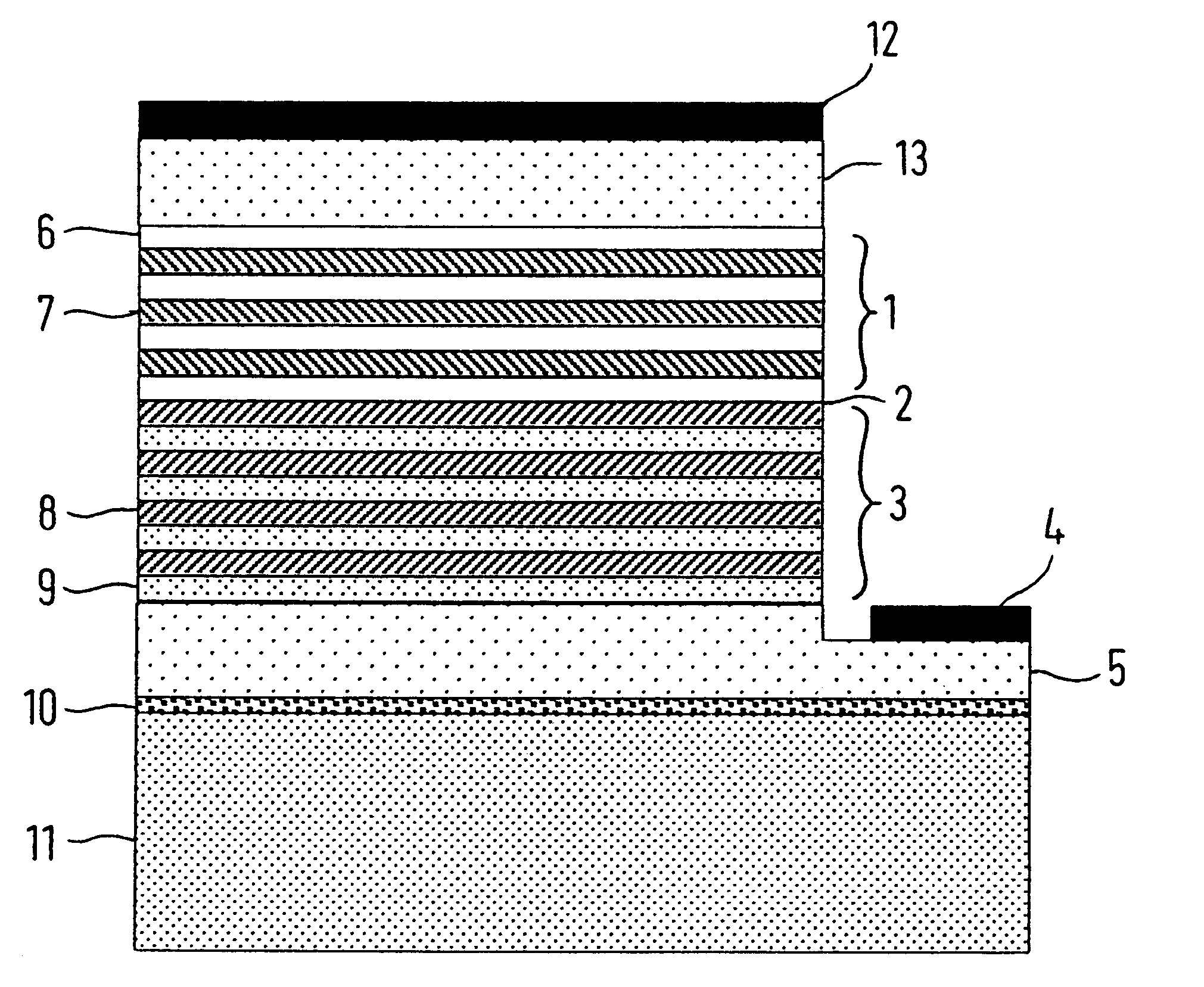
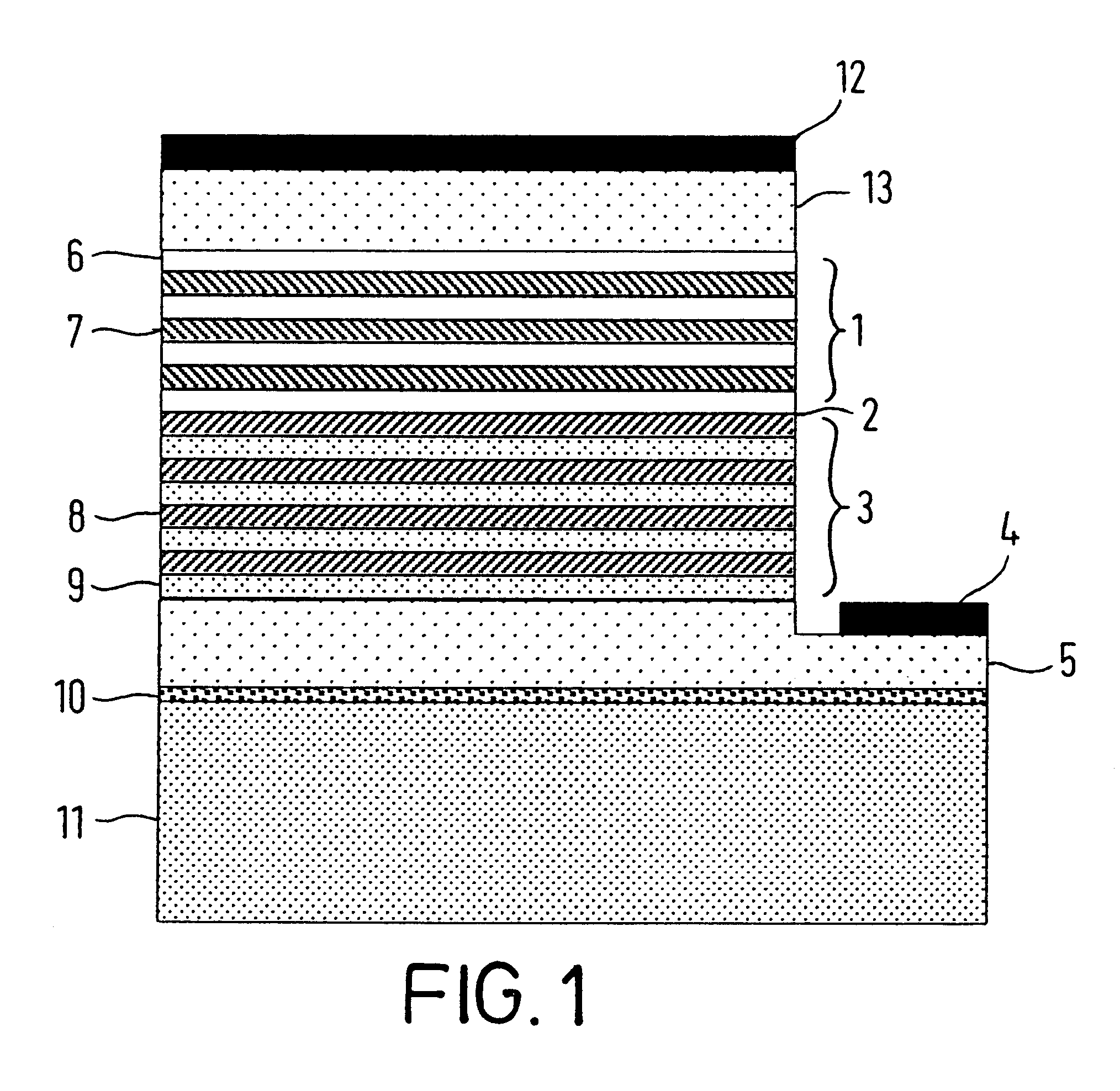
FIG. 3. shows a ULED structure according to Example 2. It has the same structure as Example 1, shown in FIG. 1, except there is an active layer 19 containing optically active impurities or Ga.sub.x Al.sub.1-x N quantum dots at the interface between the superlattices 1 and 3. The active layer allows the use of lateral quantization (LQ) related to quantum dots or impurities to suppress phonon energy relaxation channel for electrons. The use of LQ means the absence of free motion along the quantum well plane. This makes the electron energy spectrum discrete and in the case when all gaps between the levels are higher than optical phonon energy, then one-phonon transitions become forbidden by the energy conservation law.

A second advantage of the active layer is the possibility to tune resonantly the sub-band energy positions in superlattices to optically active transitions of impurities or quantum dots in the active layer. This will allow the excitation of the optical transitions in the ...

example 3

FIG. 4. shows a ULED structure for white light generation according to Example 3. It has a sapphire (Al.sub.2 O.sub.3) substrate 11 upon which an aluminium nitride (AlN) buffer layer 10 of 200 .ANG. thickness is formed. Then an n-cladding and contact layer 5 was deposited which is made of 3 .mu.m thick n-AlN doped by silicon (Si) with a doping level of 10.sup.18 -10.sup.20 cm.sup.-3. On this layer, a Gn.sub.x In.sub.y Al.sub.1-x-y N / AlN graded superlattice 20 was epitaxially grown which is formed of three undoped 5-20 .ANG. thick Ga.sub.x In.sub.y Al.sub.1-x-y N / AlN quantum wells 21 and four 10 .ANG. thick AlN barriers 22. The variations of x and y are in the range of 0.05-1.0.

Then an active layer 23 containing optically active impurities or Ga.sub.x In.sub.y Al.sub.1-x-y N quantum dots was deposited.

On the active layer 23 a Ga.sub.x In.sub.y Al.sub.1-x-y N / AlN graded superlattice 24 was epitaxially gown which is formed of three undoped 5-20 .ANG. thick Ga.sub.x In.sub.y Al.sub.1-x-...


PUM


Abstract

The fabrication of unipolar light emitting devices (ULEDs) based on III-nitride semiconductors is disclosed using an effective "p-n junction" between two n-type III-nitride semiconductor superlattices. Such a device works like a usual light emitting diode at forward bias but the radiation arises not due to recombination of electrons and holes but due to electron transitions from a shallow sub-band superlattice into a deep sub-band superlattice.

Description

1. Field of the InventionThe present invention relates to light emitting devices. More particularly, the invention relates to unipolar light emitting devices based on III-nitride semiconductors.2. Description of the Prior ArtRecent developments in the field of III-nitride semiconductors give rise to a new generation of light emitting diodes and lasers for the visible spectral range. The main advantage of nitride semiconductors in comparison with other wide-band-gap semiconductors is their low degradation in optical devices. However, there is a problem in getting a good p-type conductivity for these materials, which blocks further development of high power lasers and light emitting diodes for the visible spectral range.Various aspects of the present invention are set out below.A light emitting device with a plurality of superlattices which are made exclusively of intrinsic or n-type III-nitride semiconductors or alloys.A light emitting device with a plurality of superlattices which a...

Claims


Application Information

Patent Timeline
Patent Type & Authority Patents(United States)
IPC IPC(8): H01L33/00H01L33/06H01L33/32H01S5/343
CPCB82Y20/00H01L33/06H01L33/32
Inventor WANG, WANG NANGSHRETER, YURII GEORGIEVICHREBANE, YURII TOOMASOVICH
Owner ARIMA OPTOELECTRONICS
Why Eureka
Try Eureka