Double doped-layer, phosphorescent organic light emitting devices

a light-emitting device and organic technology, applied in the direction of discharge tube/lamp details, organic semiconductor devices, discharge tubes, etc., can solve the problems of energy loss, energy loss, and inability to convert excitons in fluorescent devices to energetically unfavorable higher singlet excited states, etc., to achieve high efficiency levels

Inactive Publication Date: 2005-03-15
THE TRUSTEES FOR PRINCETON UNIV
View PDF12 Cites 84 Cited by
  • Summary
  • Abstract
  • Description
  • Claims
  • Application Information

AI Technical Summary

Benefits of technology

The present invention is directed to phosphorescent OLEDs having a double doped-layer structure that preferably emit light in the blue range of

Problems solved by technology

The remaining excitons in a fluorescent device, which are produced in the lowest triplet excited state of an organic molecule, are typically not capable of being converted into the energetically unfavorable higher singlet excited states from which the fluorescence is produced.
This energy, thus, becomes lost to radiati

Method used


Image

  • Double doped-layer, phosphorescent organic light emitting devices
  • Double doped-layer, phosphorescent organic light emitting devices
  • Double doped-layer, phosphorescent organic light emitting devices

Examples


example 1

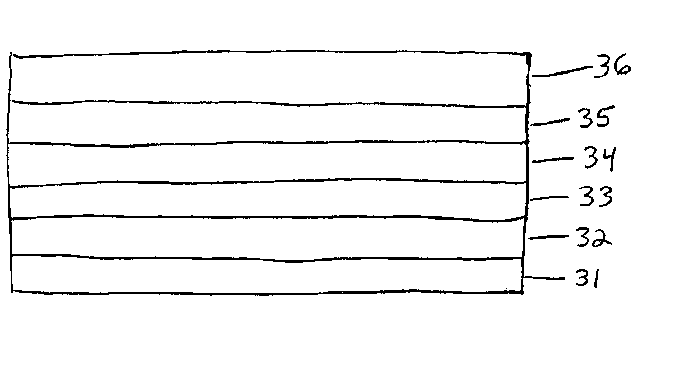
A first HTL is first deposited onto an ITO (indium tin oxide) coated glass substrate. The first HTL consists of about 400 Å of R854. A second HTL consists of about 200 Å of R854, and is deposited onto the first HTL. The second HTL is about 6% doped with Ir(4,6-F2ppy)(pico). A first ETL consists of about 200 Å of TAZ, and is deposited onto the second HTL. The first ETL is about 6% doped with Ir(4,6-F2ppy)(pico). A second ETL of Alq3 having a thickness of about 400 Å is deposited onto the first ETL. The device is finished by depositing a Mg / Ag electrode onto the second ETL. This Mg / Ag electrode has a thickness of about 100 nm. All of the depositions are carried out at a vacuum less than 5×10⁻⁵ Torr. The devices are tested in air, without packaging.

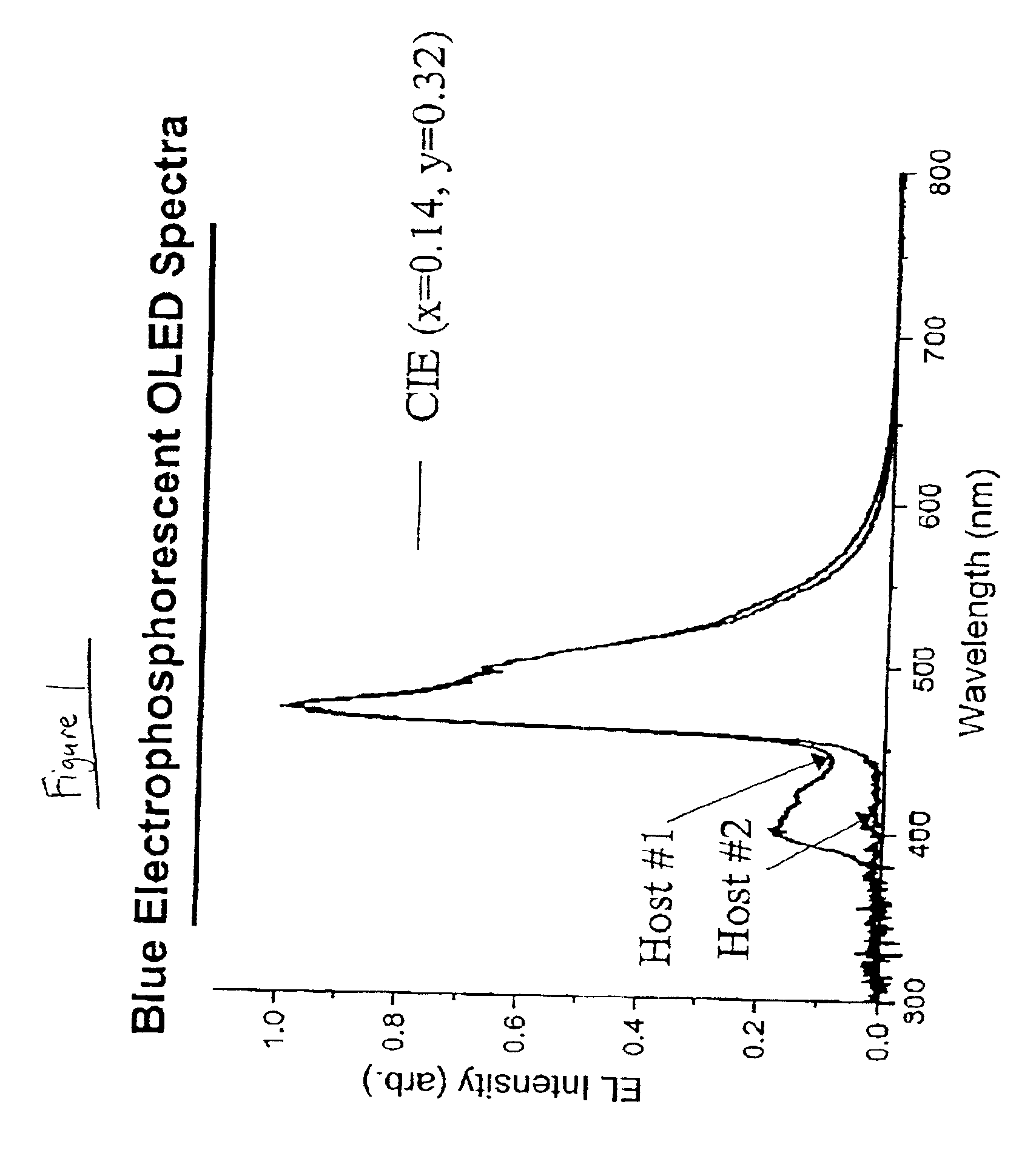
FIG. 1 shows a depiction of the EL intensity as a function of wavelength for two different OLEDs. The first OLED (Host #1) has a ITO / R854 (450 Å) / TAZ:6%-Ir(4,6-F2ppy) (pico) (250 Å) / Alq3(450 Å) / MgAg layer structure, and the second OLED (Host...


PUM


Abstract

Phosphorescent OLEDs having a double doped-layer structure wherein the OLEDs include a hole transporting layer (HTL) having a phosphorescent material doped therein, and an electron transporting layer (ETL) having the same phosphorescent material doped therein. Typically, these phosphorescent OLEDs have an anode, a first HTL over the anode, a second HTL that is doped with a phosphorescent material over the first HTL, a first ETL that is doped with a phosphorescent material over the second HTL, a second ETL over the first ETL, and a cathode over the second ETL. These phosphorescent OLEDs preferably include blue phosphorescent OLEDs with high efficiency levels.

Description

FIELD OF THE INVENTIONThe present invention is directed to double doped-layer, phosphorescent organic light emitting devices that are, for example, capable of emitting blue light. The present invention is directed to, for example, an organic light emitting device (OLED) over a substrate, where the OLED has an anode, a first hole transporting layer (HTL), a second hole transporting layer that is doped with a phosphorescent material, a first electron transporting layer (ETL) that is doped with a phosphorescent material, a second electron transporting layer, and a cathode.BACKGROUND OF THE INVENTIONOrganic light emitting devices (OLEDs), which make use of thin film materials that emit light when excited by electric current, are expected to become an increasingly popular form of flat panel display technology. This is because OLEDs have a wide variety of potential applications, including cell phones, personal digital assistants (PDAs), computer displays, informational displays in vehicle...

Claims


Application Information

Patent Timeline
IPC IPC(8): H01L51/50H01L51/30H01L51/05H01L51/00
CPCH01L51/005H01L51/5016H01L51/5048H01L51/0059H01L51/0078H01L51/0081H01L2251/308H01L51/0085H01L51/0087H01L51/0084H10K85/60H10K85/631H10K85/311H10K85/341H10K85/324H10K85/346H10K85/342H10K50/11H10K2101/10H10K50/14H10K2102/103H05B33/00H05B33/14
Inventor ADACHI, CHIHAYABALDO, MARC A.FORREST, STEPHEN R.
Owner THE TRUSTEES FOR PRINCETON UNIV
Why Eureka
Try Eureka