High frequency RF interconnect for semiconductor automatic test equipment

Inactive Publication Date: 2005-05-31
KEITHLEY INSTRUMENTS INC
View PDF19 Cites 14 Cited by
  • Summary
  • Abstract
  • Description
  • Claims
  • Application Information

AI Technical Summary

Problems solved by technology

These techniques have proven unsatisfactory for RF testing because of the tendency for the RF energy to radiate.
However, exis

Method used


Image

  • High frequency RF interconnect for semiconductor automatic test equipment
  • High frequency RF interconnect for semiconductor automatic test equipment
  • High frequency RF interconnect for semiconductor automatic test equipment

Examples


Embodiment Construction

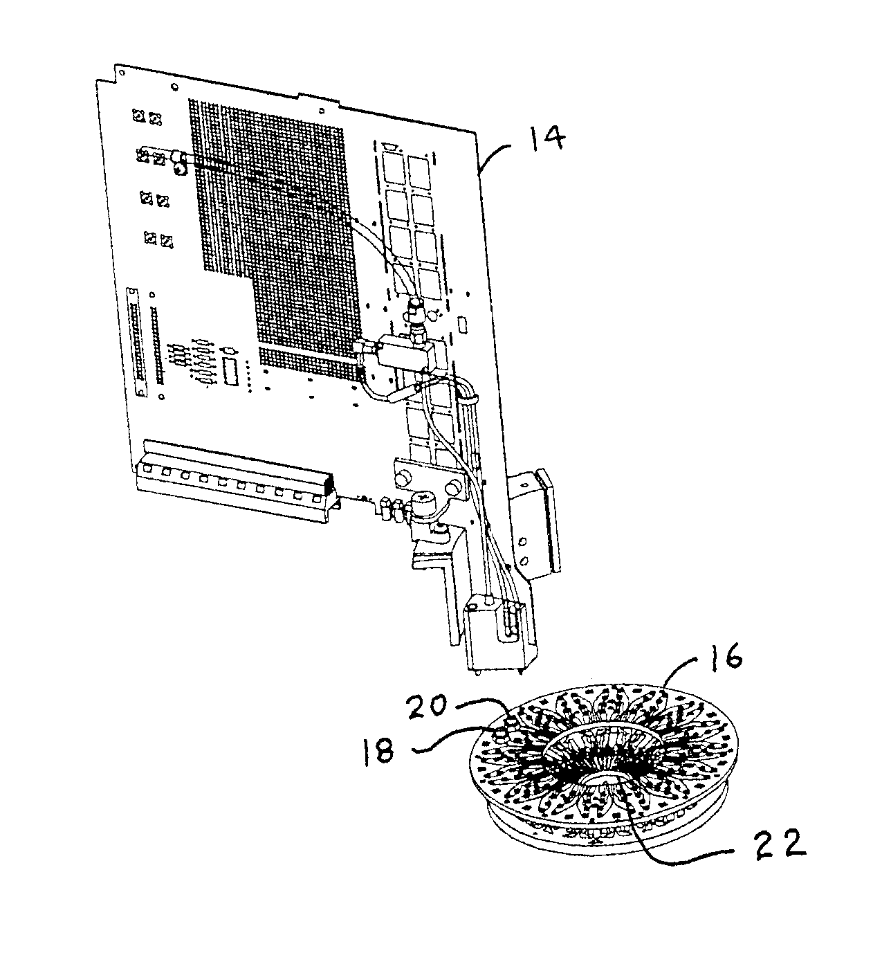
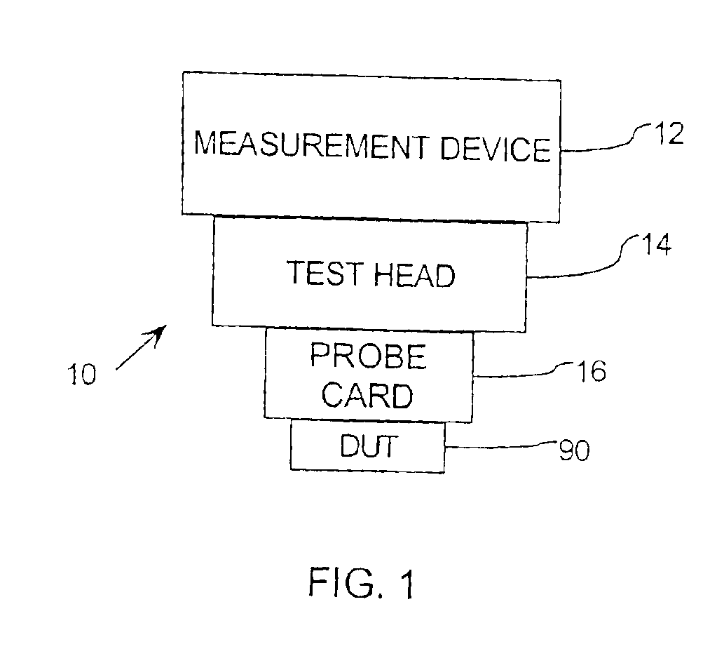
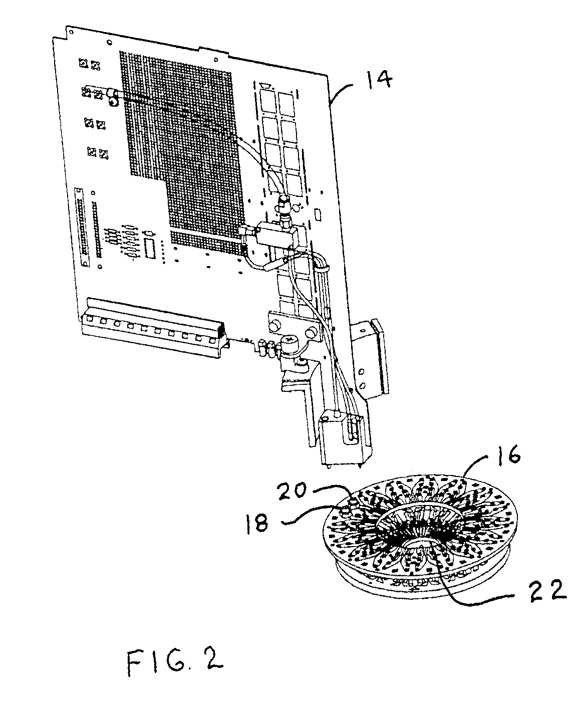
[0012]Referring to FIG. 1, a semiconductor device tester 10 for performing tests on semiconductor device includes a measurement device 12, a test head 14 and a probe card 16. The measurement device 10 performs electrical measurements on the device under test (DUT) 90.

[0013]In operation, the tester 10 is configured such that the DUT 90 is placed under the probe card 16 which contains fine electrical probes that contact points of interest on the DUT 90. Different probe cards may be conveniently configured to have probes that are arranged for different DUTs. The bottom portion of the probe card 16 has a selection and pattern of probes. The top portion of the probe card 16 has connectors that mate with the test head 14 in a more standard arrangement then that of the probes. The measurement device 12 is either contained within the test head 16 itself or is electrically connected thereto.

[0014]To allow for the rapid, trouble-free, reconfiguration of the tester 10 for the testing of a diff...


PUM


Abstract

A RF test interconnection system for connecting a measurement device to a device under test includes, a probe card having a probe extending from a first side of the card for making electrical contact with the device under test and a coaxial connector extending from a second side of the card, a test head having a test head coaxial connector that will mate with the probe card coaxial connector when the probe card and the test head are urged together, and a de-mating device attached to either the probe card or the test head for urging the probe card and the test head apart by applying a separating force therebetween. The probe card and the test card coaxial connectors are electrically connected when the test head and the probe card are urged together by a connection force and electrically disconnected when the connection force is removed.

Description

BACKGROUND OF THE INVENTION[0001]The present invention relates to automatic test equipment and, in particular, to a radio frequency interconnection system for use in connecting a device under test to a measurement device.[0002]Semiconductor devices are often tested by test equipment that includes a probe card that is configured with fine probes that make electrical contact with desired points on the semiconductor device. A differently configured probe card can be used for different semiconductor devices. The probe card is then mated with a test head that is typically able to mate with the differently configured probe cards in a uniform manner. The test head either includes or is connected to the measurement devices required to perform the desired tests on the semiconductor devices.[0003]When a different semiconductor device is to be tested, it is desirable to “drop-in” the appropriate probe card into the test equipment and connect the test head to the probe card.[0004]For non-RF tes...

Claims


Application Information

Patent Timeline
IPC IPC(8): G01R1/04G01R1/02G01R1/067G01R31/28
CPCG01R31/2889G01R1/06772
Inventor KNAUER, WILLIAM
Owner KEITHLEY INSTRUMENTS INC
Why Eureka
Try Eureka