

Image pickup module
a technology of image pickup and module, which is applied in the direction of instrumentation, color signal processing circuit, radio control device, etc., can solve the problems of image distortion, image deflection, inconvenience in design and use of products, etc., and achieve the effect of avoiding image deflection
- Summary
- Abstract
- Description
- Claims
- Application Information
AI Technical Summary
Benefits of technology
Problems solved by technology
Method used
Image

Examples
first embodiment
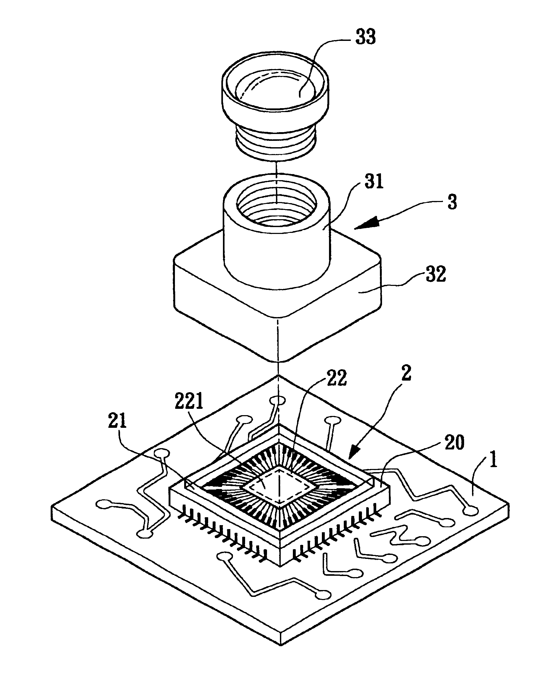
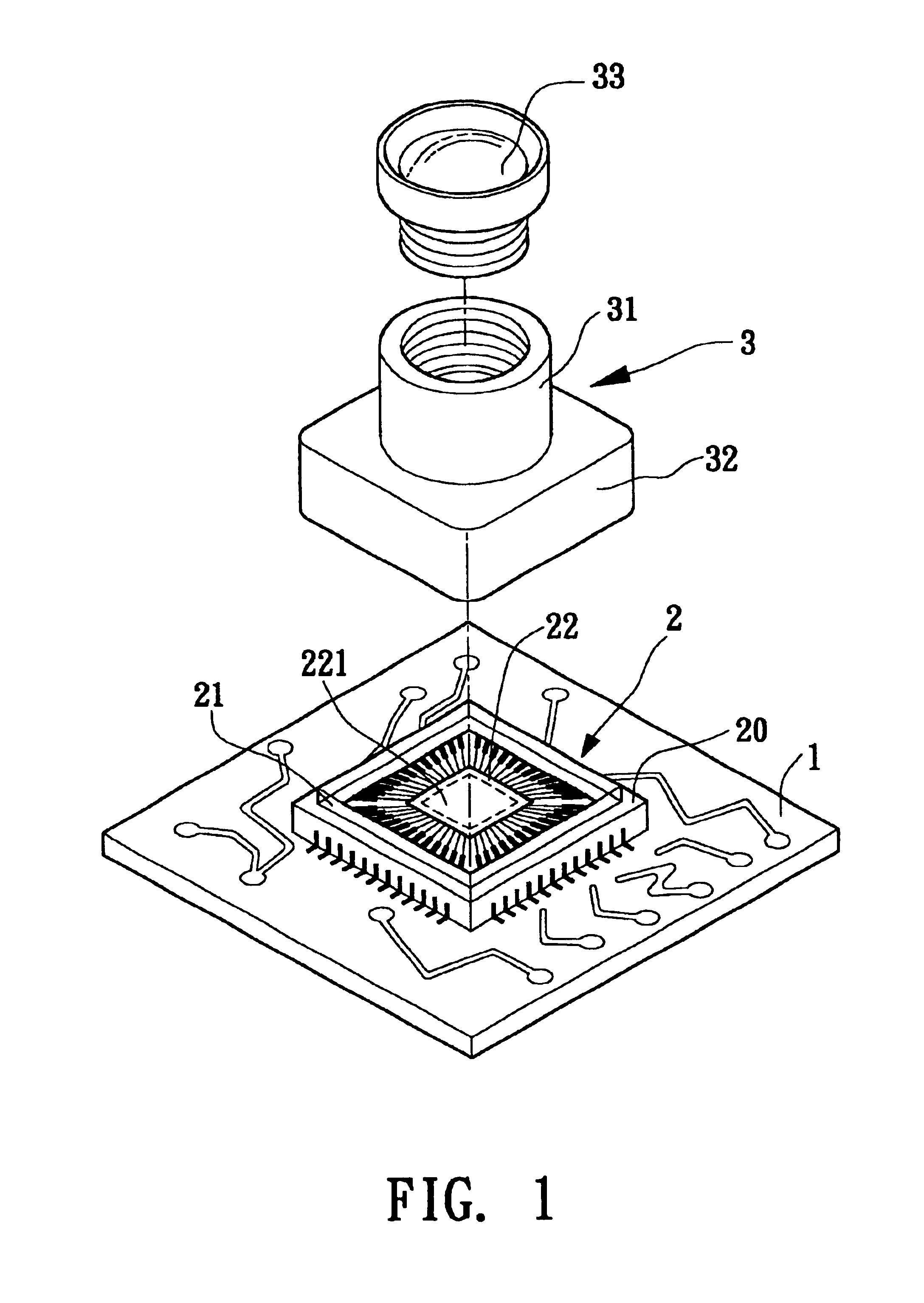
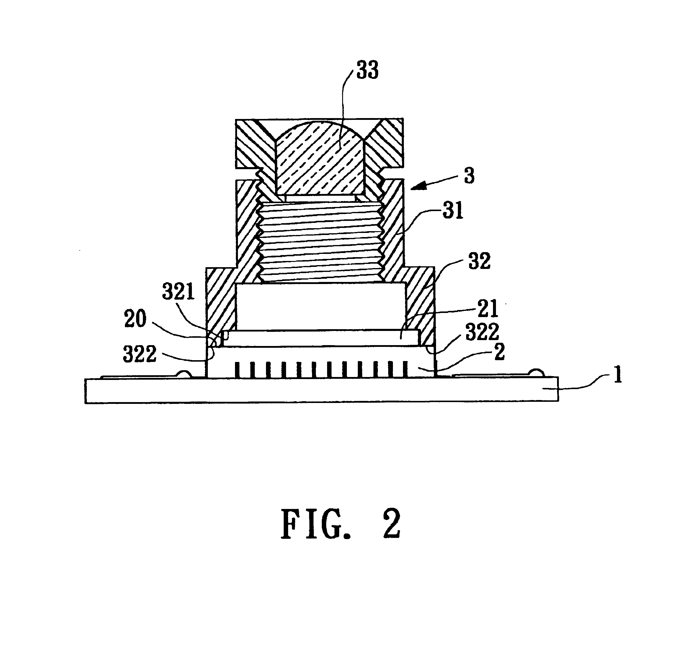
[0017]Please refer to FIGS. 1 and 2. According to the present invention, the image pickup module includes a circuit main board 1 on which an image sensor 2 (CMOS, CCD) and relevant electronic elements are laid. A lens seat 3 is disposed on the upper edge of the package of the image sensor 2.
[0018]The upper package of the image sensor 2 includes a sealing glass sheet 21. The outer periphery of the glass sheet 21 is slightly smaller than the profile of the package of the image sensor 2, whereby a plane section 20 free from covering of the glass sheet 21 is left on the periphery of top face of the image sensor 2.
[0019]The lens seat 3 has an image pickup cylinder 31 correspondingly positioned above and at least covering the coupling transistor 22 of the image sensor 2. A connecting section 32 is formed on the bottom of the image pickup cylinder 31. The outer periphery of the connecting section 32 has a dimension equal to that of the outer periphery of the image sensor 3. The inner perip...
second embodiment
[0023]FIG. 3 shows the present invention, in which the top package of the image sensor 4 (CMOS, CCD) includes a sealing glass sheet 41. The outer periphery of the glass sheet 41 is overlaid on and flush with the profile of the package of the image sensor 4. The inner periphery of the bottom face of the connecting section 32a of the lens seat is formed with a step face 321a. The inner periphery of the step face 321a has a dimension slightly smaller than that of the outer periphery of the glass sheet 41. The step face 321a is attached to the periphery of the top face of the glass sheet 41. With the profile of the outer periphery of the package of the image sensor 4 serving as a standard for the outer periphery of the step face 321a, the axis of the lens 33a is projected onto the sensor center of the coupling transistor.
third embodiment
[0024]FIG. 4 shows the present invention, in which the top package of the image sensor 5 (CMOS, CCD) includes a sealing glass sheet 51. The outer periphery of the glass sheet 51 is slightly smaller than the profile of the package of the image sensor 5. The inner periphery of the bottom face of the connecting section 32b of the lens seat is formed with a step face 321b. The inner periphery of the step face 321b has such a dimension as to encompass the entire glass sheet 51. With the profile of the outer periphery of the package of the image sensor 5 serving as a standard for the outer periphery of the step face 321b, the axis of the lens 33b is projected onto the sensor center of the coupling transistor.
PUM
 Abstract
Description
Claims
Application Information