Refresh control for semiconductor memory device

a memory device and semiconductor technology, applied in the field of refresh control, can solve the problems of affecting the operation of the refresh operation, too short activation time or pre-charge time, and the size of the dram is smaller than the dram, so as to prevent the delay of the start of the external access by the refresh operation

Inactive Publication Date: 2005-06-07
SEIKO EPSON CORP
View PDF5 Cites 10 Cited by
  • Summary
  • Abstract
  • Description
  • Claims
  • Application Information

AI Technical Summary

Benefits of technology

[0013]In this embodiment, the refresh arbiter signal is not generated in a case where the external access timing signal becomes active because of a change of an external address during a period in which the address latch signal is active. Consequently, the refresh operation is not executed and the external access execution timing signal becomes active and consequently the external access is executed, even when the refresh timing signal is generated, because the refresh execution timing signal does not become active. Accordingly, in a case where the external address changes during the active period of the address latch signal, the delay of the start of the external access by the refresh operation can be prevented.

Problems solved by technology

The SRAM does not require any refreshing operation and is easily handled, but is more expensive and has a smaller capacity than the DRAM.
In the case where the pre-charge time is insufficient, the data destruction also may occur.
The too short activation time or pre-charge time may occur when skew occurs in the address transferred from the external device.

Method used


Image

  • Refresh control for semiconductor memory device
  • Refresh control for semiconductor memory device
  • Refresh control for semiconductor memory device

Examples


Embodiment Construction

[0028]Preferred exemplary embodiments of the invention are described below.

A. Terminal Structure of Semiconductor Memory Device and Outline of Working Status

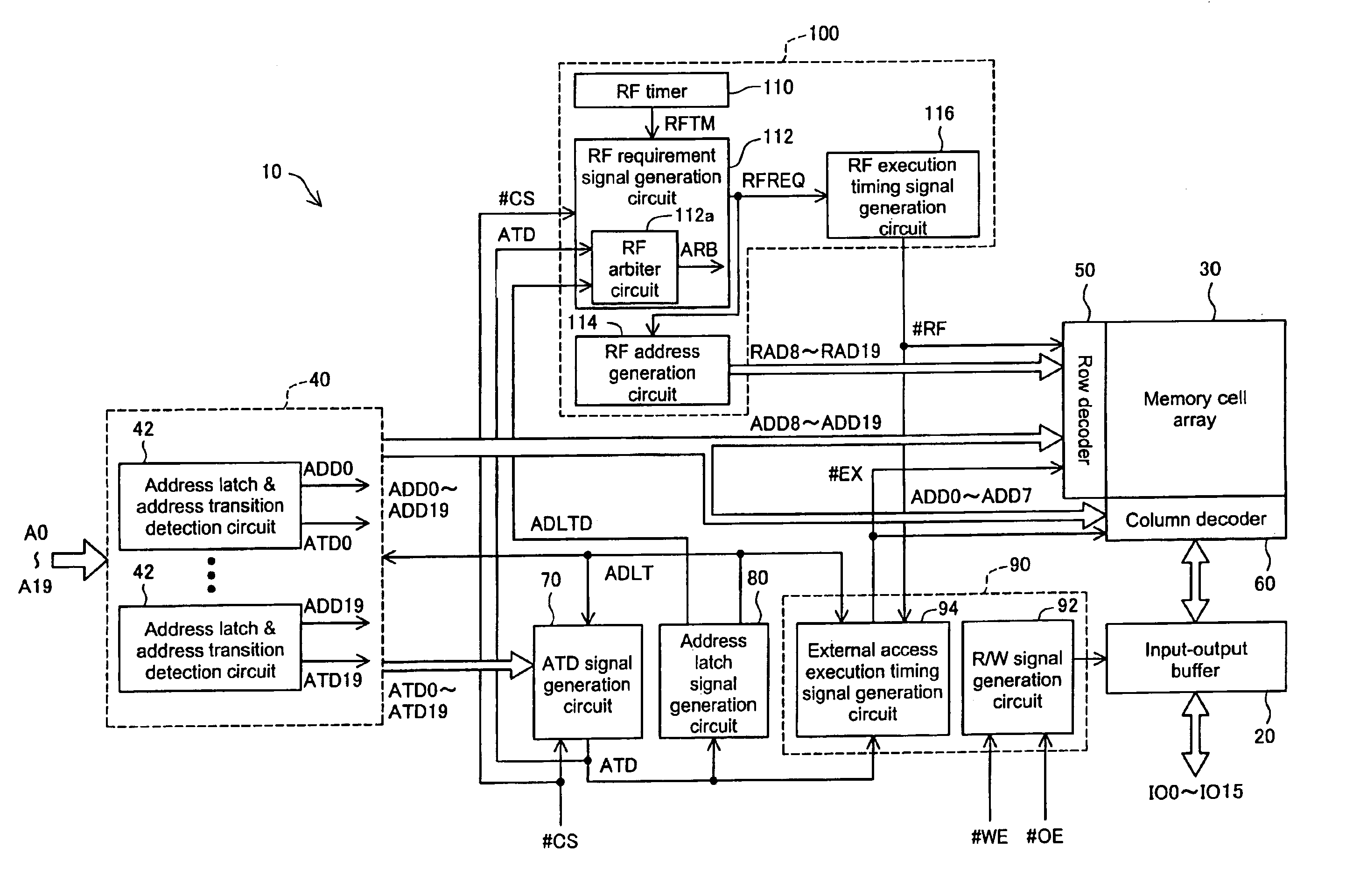
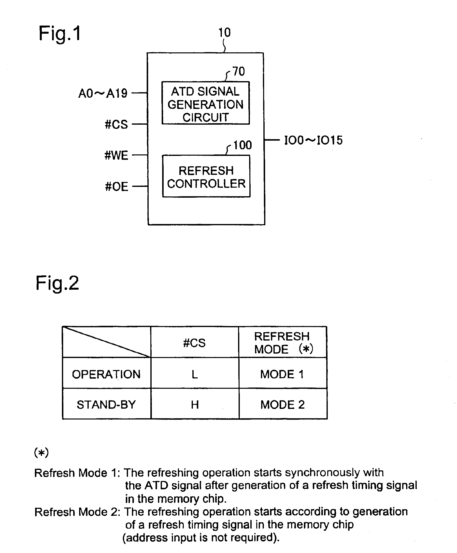
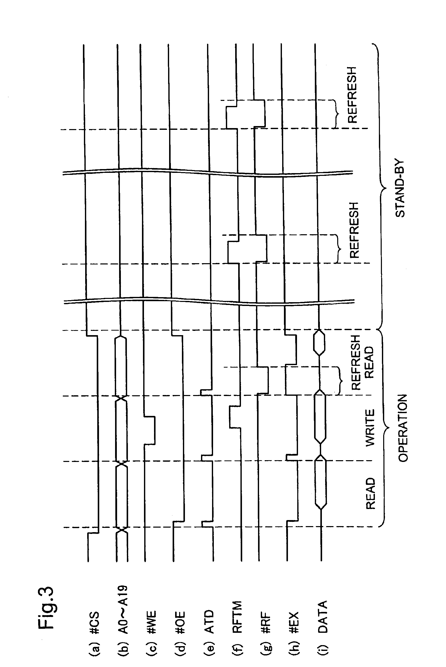
[0029]FIG. 1 schematically illustrates the terminal structure of a memory chip 10 according to one embodiment of a semiconductor memory device of the present invention. The memory chip 10 has multiple terminals given below:

[0030]A0 through A19: (20) Address input terminals

[0031]#CS: Chip select input terminal

[0032]#WE: Write enable input terminal

[0033]#OE: Output enable input terminal (Output enable signal input terminal)

[0034]IO0 through IO15: (16) Input-output data terminals

[0035]In the description hereafter, an identical symbol is assigned commonly for both the terminal name and the signal name. The prefix ‘#’ attached to the head of each terminal name (signal name) represents negative logic. Although there are multiple address input terminals A0 through A19 and multiple input-output data terminals IO0 through IO15, they are ...


PUM


Abstract

An external access timing signal becomes active according to changes of the external address. An address latch signal becomes active according to the timing when the external access timing signal becomes active. In a case where the changes of the external address occurs while the address latch signal is active and consequently the external access timing signal becomes active, a refresh arbiter signal does not become active. When the refresh arbiter signal becomes active after the generation of the refresh timing signal, a refresh execution timing signal becomes active according to the change of the refresh arbiter signal. The time period when the address latch signal is active is set to be substantially the same as the preferable activation time period. The time period when the external access timing signal is active is set to be substantially the same as the preferable pre-charge time period.

Description

BACKGROUND OF THE INVENTION[0001]1. Field of the Invention[0002]This invention relates to a semiconductor memory device equipped with a memory cell array in which dynamic memory cells are arrayed, for example, in a matrix, and in particular to a technique for providing resistance to skew in a semiconductor memory device in spite of skew in the address transferred from an external device.[0003]2. Description of Related Art[0004]Typical examples of a semiconductor memory device include a DRAM and a SRAM. As is well known, the DRAM is more affordable in price and has a larger capacity than the SRAM, but requires a refreshing operation. The SRAM does not require any refreshing operation and is easily handled, but is more expensive and has a smaller capacity than the DRAM.[0005]A virtual static RAM (called VSRAM) is a known semiconductor memory device having the advantages of the DRAM and the SRAM. The virtual SRAM (sometimes also called PSRAM, Pseudo Static RAM) has a memory cell array ...

Claims


Application Information

Patent Timeline
Patent Type & Authority Patents(United States)
IPC IPC(8): G11C11/406G11C11/403G11C11/408
CPCG11C11/406G11C11/40615G11C11/40603
Inventor MIZUGAKI, KOICHI
Owner SEIKO EPSON CORP
Why Eureka
Try Eureka