Method and apparatus of generating PDMAT precursor

a technology of pdmat and precursor, which is applied in the direction of crystal growth process, sublimation, separation process, etc., can solve the problems of compromising device integrity, affecting the integrity of devices, and affecting the quality of pdmat precursors,

Inactive Publication Date: 2005-06-14
APPLIED MATERIALS INC
View PDF62 Cites 124 Cited by
  • Summary
  • Abstract
  • Description
  • Claims
  • Application Information

AI Technical Summary

Benefits of technology

[0012]Embodiments of the present invention further include purified pentakis(dimethylamido)tantalum having less than about 5 ppm of chlorine.

Problems solved by technology

However, as the fringes of circuit technology are pressed, the shrinking dimensions of interconnects in VLSI and ULSI technology have placed additional demands on the processing capabilities.
Many traditional deposition processes have difficulty filling sub-micron structures where the aspect ratio exceeds 4:1, and particularly where the aspect ratio exceeds 10:1.
Therefore, there is a great amount of ongoing effort being directed at the formation of substantially void-free and seam-free sub-micron features having high aspect ratios.
However, one problem with the use of copper is that copper diffuses into silicon, silicon dioxide, and other dielectric materials which may compromise the integrity of devices.
However, the chemicals used in the barrier layer deposition, such as pentakis(dimethylamido) tantalum (PDMAT; Ta[NH2(CH3)2]5), may include impurities that cause defects in the fabrication of semiconductor devises and reduce process yields.

Method used


Image

  • Method and apparatus of generating PDMAT precursor
  • Method and apparatus of generating PDMAT precursor
  • Method and apparatus of generating PDMAT precursor

Examples


Embodiment Construction

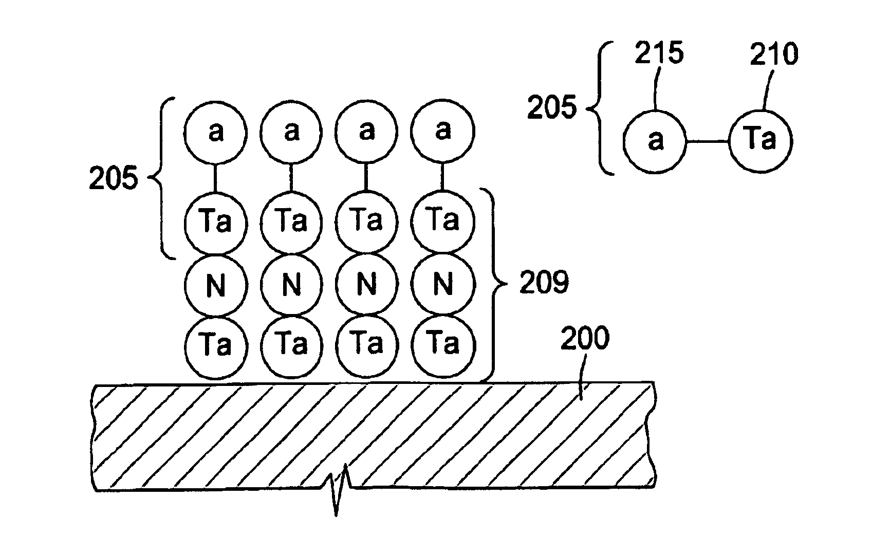
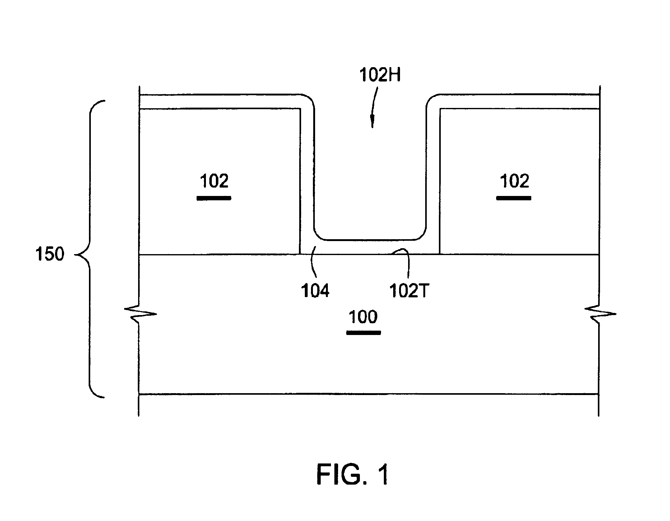
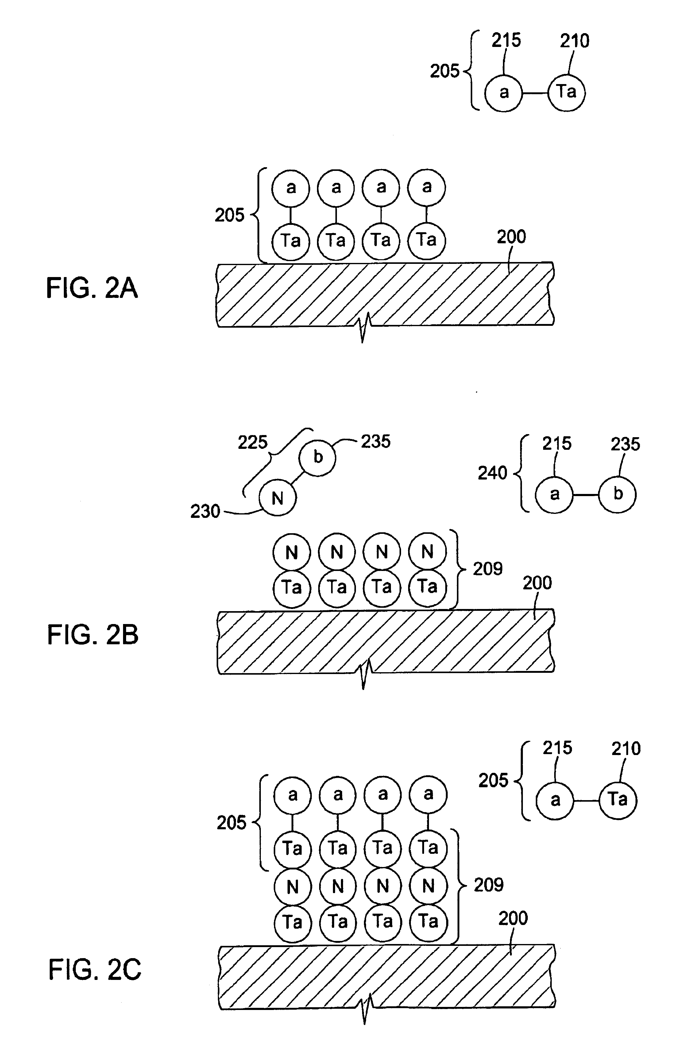
[0023]FIG. 1 is a schematic cross-sectional view of one embodiment of a substrate 100 having a dielectric layer 102 and a barrier layer 104 deposited thereon. Depending on the processing stage, the substrate 100 may be a silicon semiconductor substrate, or other material layer, which has been formed on the substrate. The dielectric layer 102 may be an oxide, a silicon oxide, carbon-silicon-oxide, a fluoro-silicon, a porous dielectric, or other suitable dielectric formed and patterned to provide a contact hole or via 102H extending to an exposed surface portion 102T of the substrate 100. For purposes of clarity, the substrate 100 refers to any work piece upon which film processing is performed, and a substrate structure 150 is used to denote the substrate 100 as well as other material layers formed on the substrate 100, such as the dielectric layer 102. It is also understood by those with skill in the art that the present invention may be used in a dual damascene process flow. The ba...


PUM

PropertyMeasurementUnit
temperatureaaaaaaaaaa
pressureaaaaaaaaaa
thicknessaaaaaaaaaa

Abstract

A precursor and method for filling a feature in a substrate. The method generally includes depositing a barrier layer, the barrier layer being formed from pentakis(dimethylamido)tantalum having less than about 5 ppm of chlorine. The method additionally may include depositing a seed layer over the barrier layer and depositing a conductive layer over the seed layer. The precursor generally includes pentakis(dimethylamido)tantalum having less than about 5 ppm of chlorine. The precursor is generated in a canister having a surrounding heating element configured to reduce formation of impurities.

Description

CROSS-REFERENCE TO RELATED APPLICATIONS[0001]This application is a continuation-in-part of co-pending U.S. patent application Ser. No. 10 / 198,727 (AMAT / 6798) filed Jul. 17, 2002, which is incorporated herein by reference.BACKGROUND OF THE INVENTION[0002]1. Field of the Invention[0003]The present invention generally relates to depositing a barrier layer on a semiconductor substrate.[0004]2. Description of the Related Art[0005]Reliably producing sub-micron and smaller features is one of the key technologies for the next generation of very large scale integration (VLSI) and ultra large scale integration (ULSI) of semiconductor devices. However, as the fringes of circuit technology are pressed, the shrinking dimensions of interconnects in VLSI and ULSI technology have placed additional demands on the processing capabilities. The multilevel interconnects that lie at the heart of this technology require precise processing of high aspect ratio features, such as vias and other interconnects...

Claims


Application Information

Patent Timeline
Patent Type & Authority Patents(United States)
IPC IPC(8): C23C16/448C23C16/44C23C16/34C23C16/18C23C16/455H01L21/31
CPCC23C16/18C23C16/34C23C16/4402C23C16/4481C23C16/4487C23C16/45544C23C16/4482Y10T117/1008Y10T117/10Y10T117/1004B01D7/00C23C16/448C23C16/52H01L21/67207
Inventor CHEN, LINGKU, VINCENT W.CHUNG, HUAMARCADAL, CHRISTOPHEGANGULI, SESHADRILIN, JENNYWU, DIEN-YEHOUYE, ALANCHANG, MEI
Owner APPLIED MATERIALS INC
Why Eureka
Try Eureka