Partial reconfiguration of a programmable logic device using an on-chip processor

a programmable logic and on-chip processor technology, applied in the direction of computation using denominational number representation, pulse technique, instruments, etc., can solve the problems of limiting the flexibility of the partial reconfiguration process, inefficient storage of configuration data values in two separate external memories, and inconvenient operation

a programmable logic and on-chip processor technology, applied in the direction of computation using denominational number representation, pulse technique, instruments, etc., can solve the problems of limiting the flexibility of the partial reconfiguration process, inefficient storage of configuration data values in two separate external memories, and inconvenient operation

US6907595B2Inactive Publication Date: 2005-06-14XILINX INC

Image

  • Partial reconfiguration of a programmable logic device using an on-chip processor
  • Partial reconfiguration of a programmable logic device using an on-chip processor
  • Partial reconfiguration of a programmable logic device using an on-chip processor

Examples


Embodiment Construction

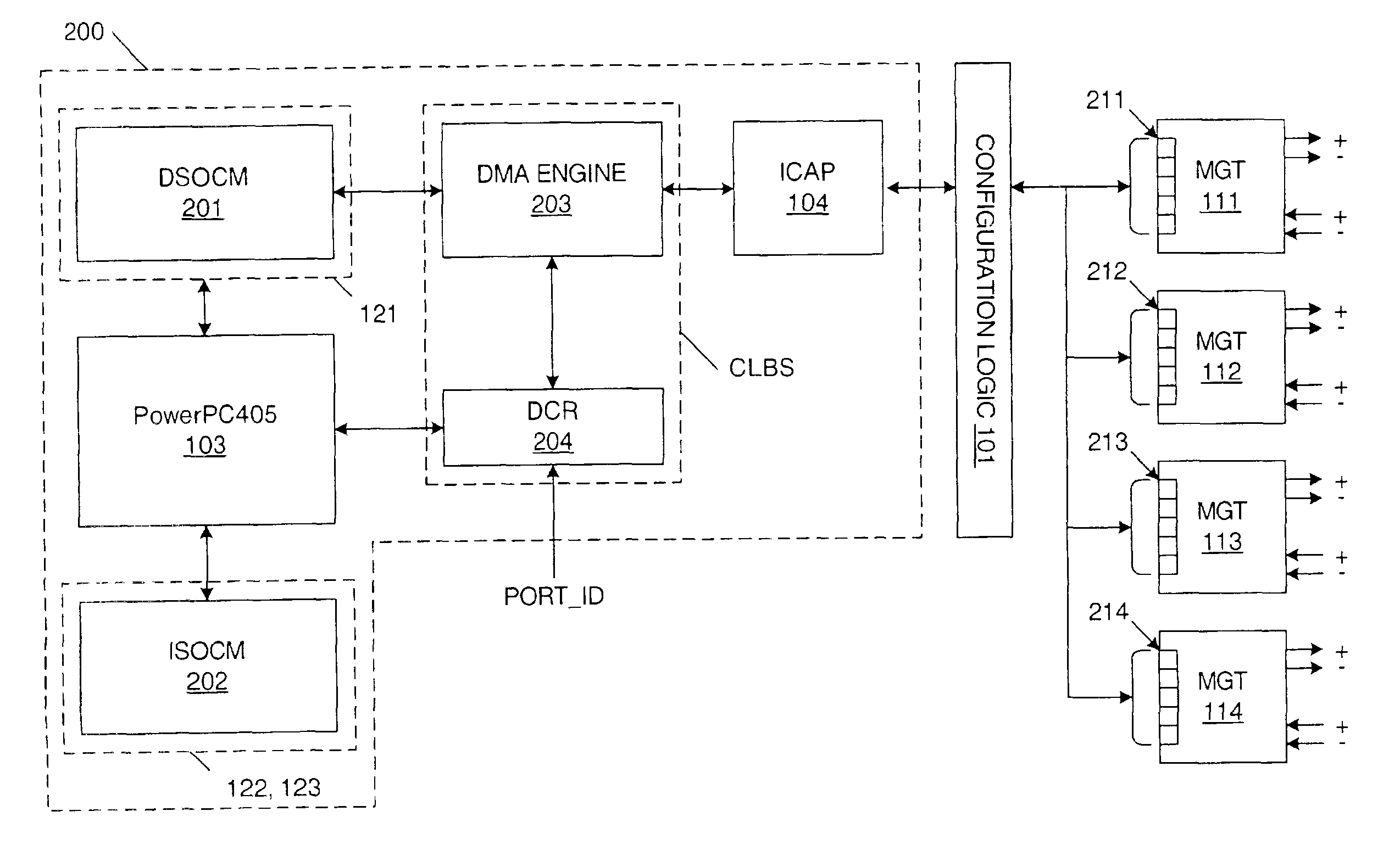
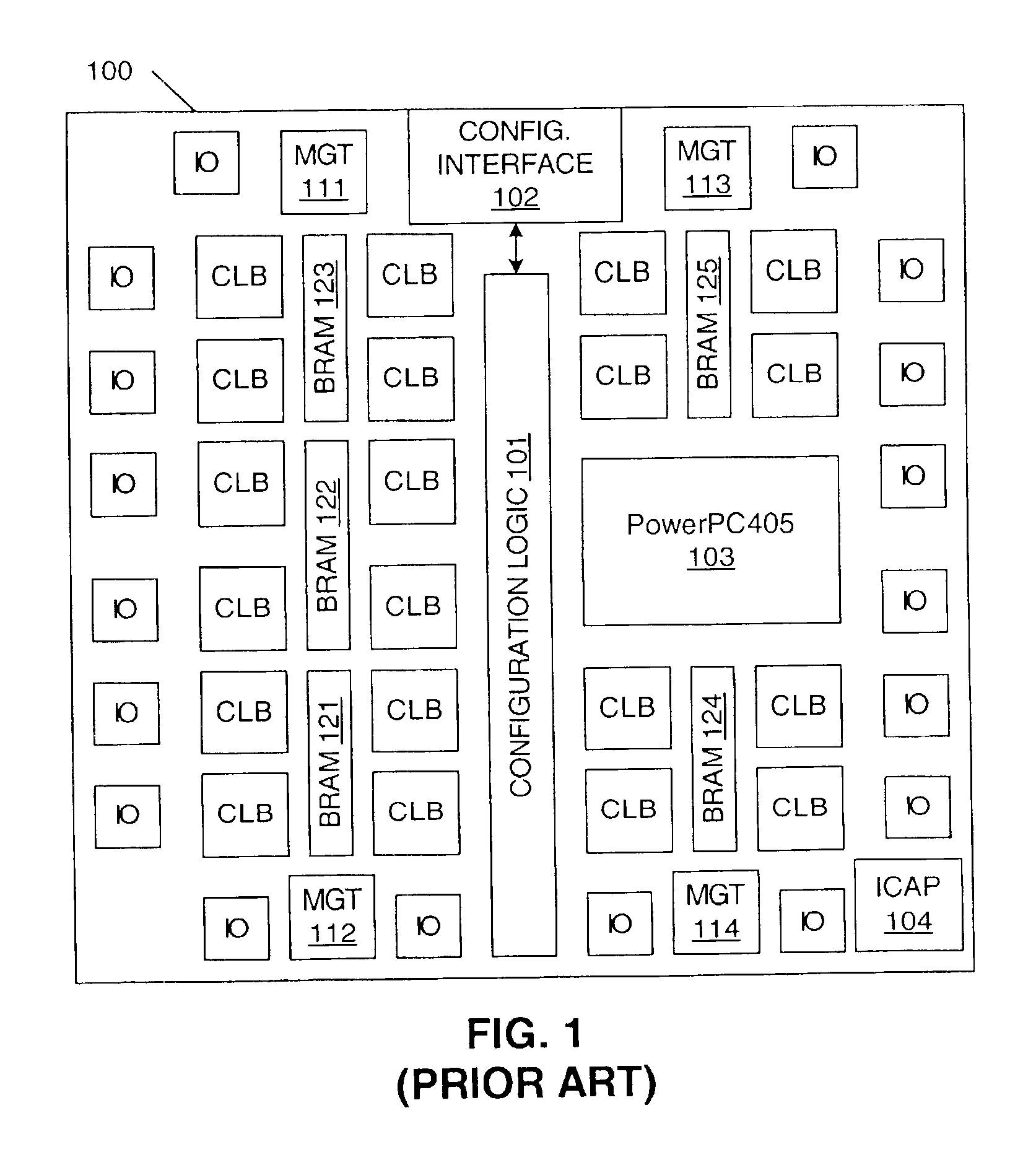
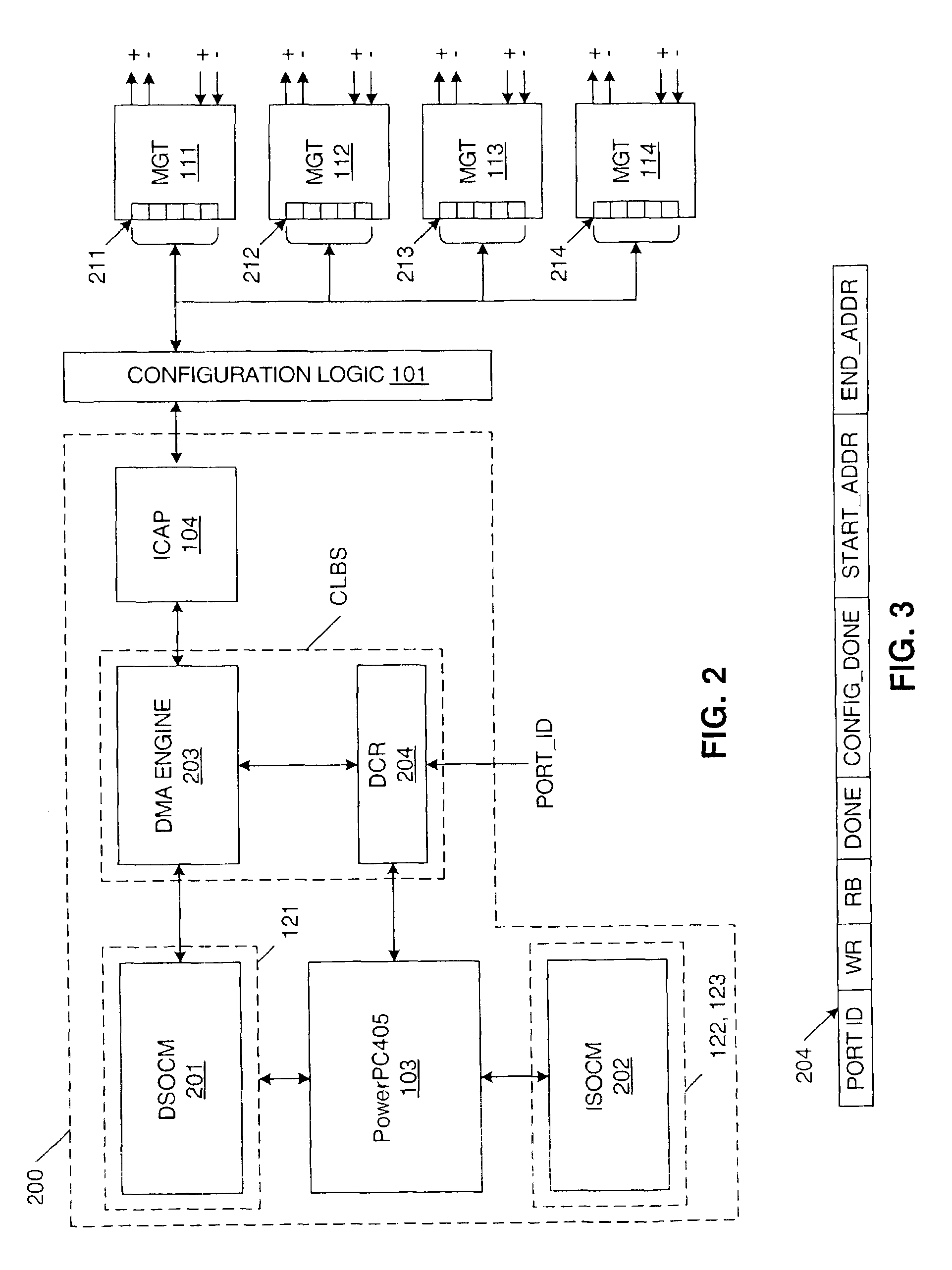
[0023]In accordance with the described embodiments of the present invention, a programmable logic device having an on-chip processor is configured to implement an efficient partial reconfiguration scheme. In the described embodiments, a conventional Virtex-IIâ„¢ Pro FPGA, available from Xilinx, Inc., is used to implement the partial reconfiguration scheme. Thus, the present invention is described in connection with the use of FPGA 100 (FIG. 1). Although the present invention is described in connection with the partial reconfiguration of FPGAs, it is understood that the partial reconfiguration scheme of the present invention may also be implemented using other programmable logic devices.

[0024]The partial reconfiguration scheme is described in connection with the partial reconfiguration of the multi-gigabit transceivers (MGTs) 111-114 of FPGA 100. However, it is understood that other elements of FPGA 100 can be partially reconfigured in accordance with the principles described below.

[00...


PUM


Abstract

A programmable logic device, such as a field programmable gate array, is partially reconfigured using a read-modify-write scheme that is controlled by a processor. The partial reconfiguration includes (1) loading a base set of configuration data values into a configuration memory array of the programmable logic device, thereby configuring the programmable logic device; (2) reading a first frame of configuration data values from the configuration memory array; (3) modifying a subset of the configuration data values in the first frame of configuration data values, thereby creating a first modified frame of configuration data values; and (4) overwriting the first frame of configuration data values in the configuration memory array with the first modified frame of configuration data values, thereby partially reconfiguring the programmable logic device. The steps of reading, modifying and overwriting are performed under the control of a processor.

Description

FIELD OF THE INVENTION[0001]The present invention relates to partial reconfiguration of a programmable logic device, such as a field programmable gate array (FPGA). More specifically, the present invention relates to the partial reconfiguration of a programmable logic device using an on-chip processor to perform a read-modify-write flow to the configuration data.RELATED ART[0002]FIG. 1 is a block diagram of a conventional FPGA 100, which includes input / output (I / O) blocks (each labeled IO) located around the perimeter of the FPGA, multi-gigabit transceivers (MGT) 111-114 interspersed with the I / O blocks, configurable logic blocks (each labeled CLB) arranged in an array, block random access memory (BRAM) 121-125 interspersed with the CLBs, configuration logic 101, configuration interface 102, on-chip processor 103 and internal configuration access port (ICAP) 104. Although FIG. 1 shows a relatively small number of I / O blocks, CLBs and block RAMs for illustration purposes. It is under...

Claims


Application Information

Patent Timeline
14 Jun 2005
Publication
US6907595B2
IPC
G06F15/76; G06F15/78
CPC
G06F15/7867
Inventors
CURD, DEREK R.; KALRA, PUNIT S.