EEPROM and EEPROM manufacturing method

a technology of floating gate and manufacturing method, which is applied in the direction of semiconductor devices, electrical devices, transistors, etc., can solve the problems of low overwriting speed, so as to reduce the dispersion of memory transistor characteristics, suppress the reduction of overwriting life and deterioration of charge holding characteristics, and the effect of superior eeprom

Inactive Publication Date: 2005-07-05
DENSO CORP
View PDF8 Cites 25 Cited by
  • Summary
  • Abstract
  • Description
  • Claims
  • Application Information

AI Technical Summary

Benefits of technology

[0015]It is therefore an object of the present invention to provide a superior EEPROM and a manufacturing method thereof. It is an another object of the present invention to provide a EEPROM and a manufacturing method thereof with which it is possible to suppress reduction of overwriting life and deterioration of charge holding characteristic while reducing dispersion of memory transistor characteristics and reducing parasitic capacitance.
[0016]A memory transistor of the EEPROM according to the present invention has a drain region comprised of an embedded layer and a drain side field moderating layer. A floating gate electrode is formed not to cover the drain side field moderating. As a result, the region where the drain region and the floating gate electrode 8 overlap is small. Therefore, the parasitic capacitance between the floating gate electrode and the drain region can be reduced.
[0017]A floating gate electrode is formed to have a gate length approximately equal to a length of a channel region between the drain region and a source region. These drain region and source region are formed self-aligningly by ion implantation with the floating gate electrode used as a mask. As a result, dispersion of the channel length can be suppressed, and therefore dispersion of memory transistor characteristics can be reduced.
[0018]Also, the floating gate entirely is formed to cover a tunnel film formed in a gate insulating film above the embedded layer. Therefore, at the time of etching for forming the floating gate electrode, the tunnel film 6 does not become exposed. By this means, the tunnel film can be prevented from suffering etching damage. Thus, it is possible to reduce deterioration of tunnel film quality and increase overwriting life.

Problems solved by technology

Consequently, there has been the problem that dispersion tends to arise in the transistor characteristics.
Consequently, there has been the problem that the overwriting speed is low.
However, even with the technology shown in FIG. 20, there are the following problems.
Consequently, the problem arises that deterioration of the tunnel film 34 occurs and the overwriting life of the device falls.
When etching damage from the working mentioned above remains on these exposed end faces, the problem arises that, because the charge of the floating gate electrode 35 escapes through these damaged end faces, the charge holding characteristic deteriorates.

Method used


Image

  • EEPROM and EEPROM manufacturing method
  • EEPROM and EEPROM manufacturing method
  • EEPROM and EEPROM manufacturing method

Examples


Embodiment Construction

[0041](First Preferred Embodiment)

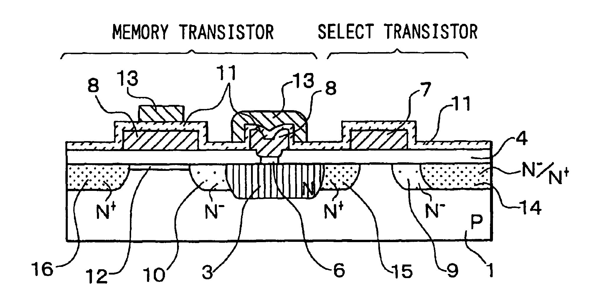
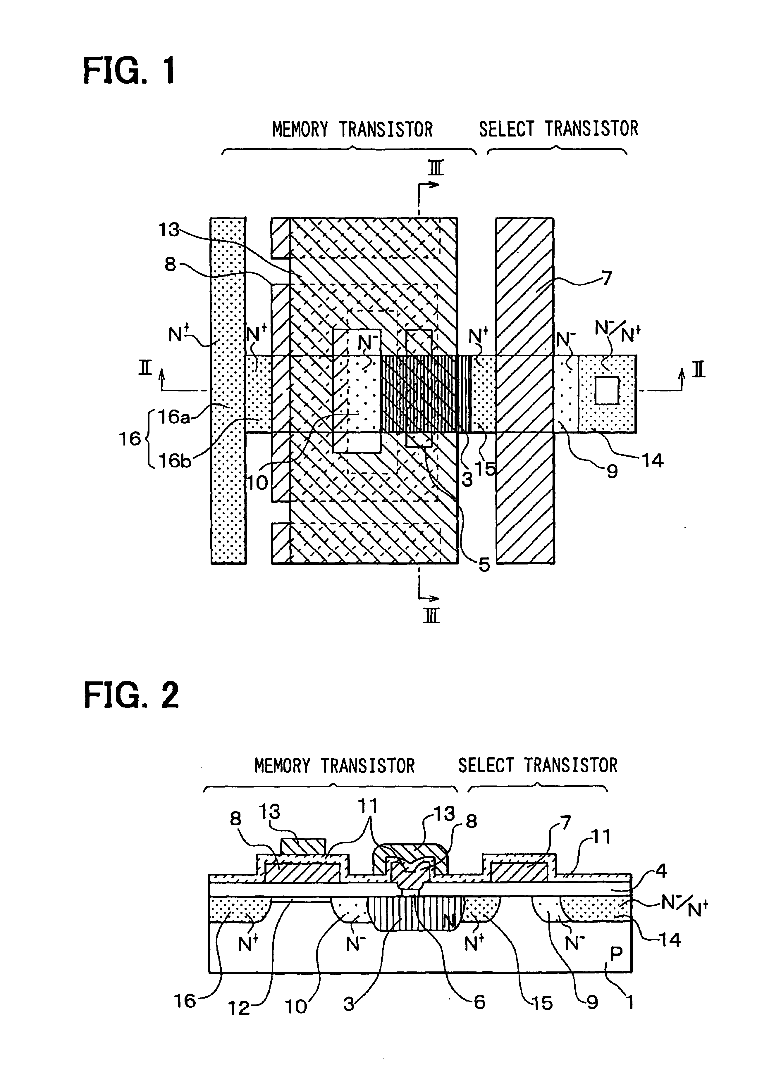
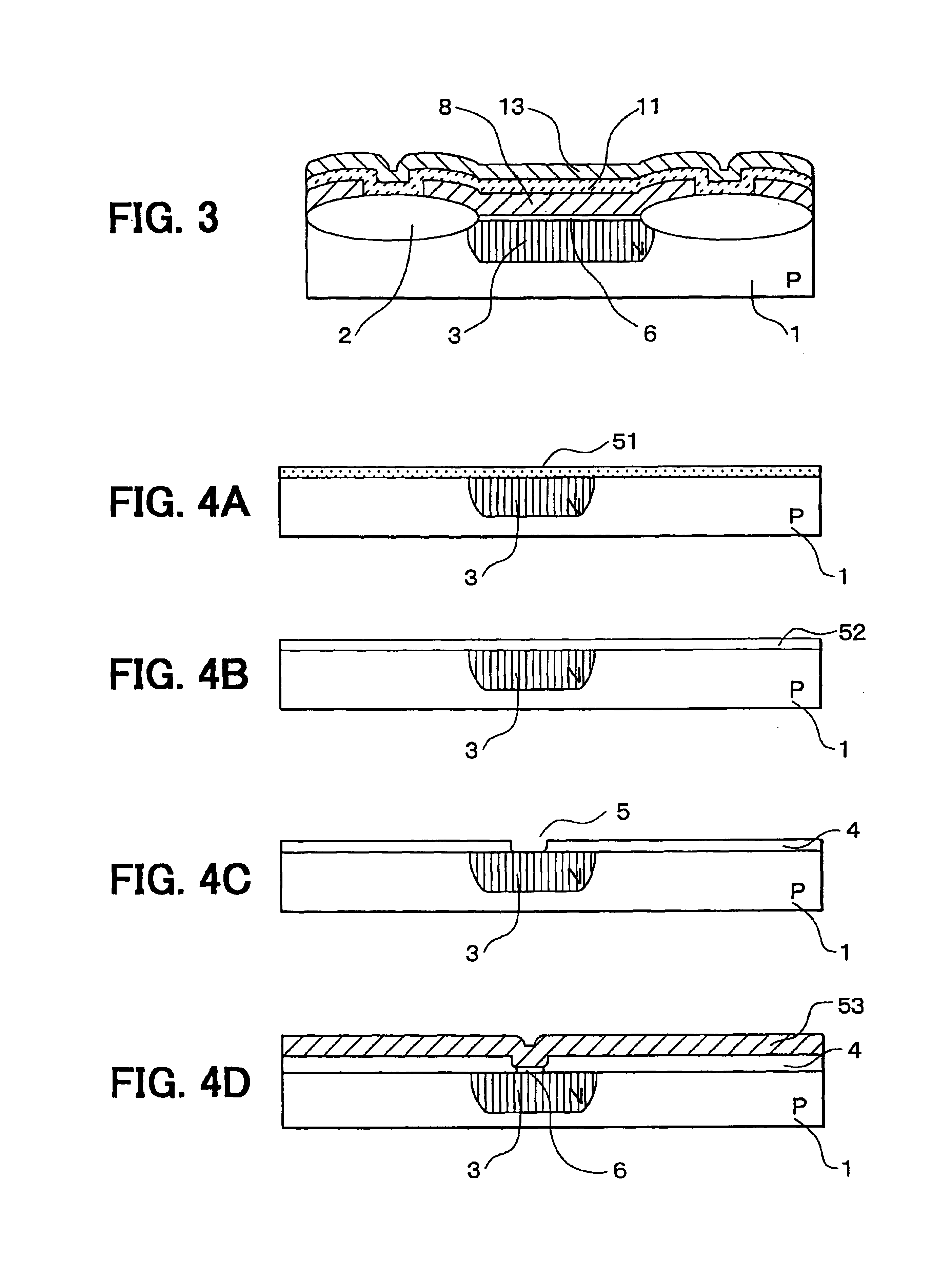
[0042]A plan view of an EEPROM of a first preferred embodiment of the invention is shown in FIG. 1, a sectional view along the line II—II in FIG. 1 is shown in FIG. 2, and a sectional view along the line III—III in FIG. 1 is shown in FIG. 3. The hatching in FIG. 1 has been added to show different regions.

[0043]The EEPROM of this preferred embodiment has a memory transistor and a select transistor.

[0044]In the memory transistor region, as shown in FIG. 2, an N-type embedded layer 3 and an N−-type drain side field moderating layer 10 and an N+-type source leadout layer 16 are formed in a superficial layer of a P-type semiconductor substrate 1 made of silicon. A tunnel film 6 is formed above the embedded layer 3, and a gate oxide film 4 is formed on the rest of the surface of the semiconductor substrate 1. A floating gate electrode 8 is formed on the tunnel film 6 and on the region between the field moderating layer 10 and the N+-type source leadout la...


PUM


Abstract

A memory transistor of an EEPROM has a floating gate electrode of a shape such that it covers the entirety of a tunnel film and a channel region and does not cover a region between the channel region and an embedded layer. And, a control gate electrode is formed on an interlayer insulating film on the floating gate electrode into a shape such that it is wider than the floating gate electrode above the tunnel film, and is narrower than the floating gate electrode above the channel region.

Description

CROSS REFERENCE TO RELATED APPLICATION[0001]This application is related to and incorporates herein by reference Japanese Patent Applications No. 2002-296066 filed on Oct. 9, 2002.FIELD OF THE INVENTION[0002]This invention relates to an electrically programmable and electrically erasable floating gate type nonvolatile memory device, and particularly to an EEPROM (Electrically Erasable Programmable Read Only Memory) in which overwriting is carried out using a Fowler Nordheim tunnel effect, and to a manufacturing method thereof.BACKGROUND OF THE INVENTION[0003]The construction of an EEPROM proposed in related art is shown in FIG. 19. The EEPROM shown in FIG. 19 has a memory transistor and a select transistor for selecting this memory transistor at times of memory overwriting and reading.[0004]In a region of the memory transistor, an embedded N-type layer 32 corresponding to a drain region and an N+-type source layer 42 are formed in a superficial layer of a semiconductor substrate 31. ...

Claims


Application Information

Patent Timeline
Patent Type & Authority Patents(United States)
IPC IPC(8): H01L27/115H01L21/70H01L29/423H01L29/40H01L21/8247H01L29/788H01L29/792
CPCH01L27/115H01L27/11521H01L27/11524H01L29/42324H10B69/00H10B41/30H10B41/35
Inventor ITOU, HIROYASUKATADA, MITSUTAKAMURAMOTO, HIDETOSHI
Owner DENSO CORP
Why Eureka
Try Eureka