Methods of forming channels on an integrated circuit die and die cooling systems including such channels

a technology of integrated circuits and cooling systems, which is applied in the direction of electrical apparatus, semiconductor devices, semiconductor/solid-state device details, etc., can solve the problems of pushing the limits of conventional cooling systems, increasing power dissipation of microprocessors and other processing devices, and damage and/or degradation of die performan

Inactive Publication Date: 2005-07-19
INTEL CORP
View PDF1 Cites 65 Cited by
  • Summary
  • Abstract
  • Description
  • Claims
  • Application Information

AI Technical Summary

Problems solved by technology

The power dissipation of microprocessors and other processing devices generally increases with each design generation, as the operating frequencies of these devices are ratcheted upwards.
Also, the design and operating conditions for a die may lead to “hot spots” on the die where the local temperature is significantly greater than in surrounding regions on the die, and a failure to adequately extract heat from such hot spots may lead to damage and / or a degradation in performance of the die.
Thus, the thermal performance of die cooling systems in future generations of IC devices will become increasingly critical, and the thermal performance required for these devices may push the limits of the conventional cooling system illustrated in FIG.

Method used


Image

  • Methods of forming channels on an integrated circuit die and die cooling systems including such channels
  • Methods of forming channels on an integrated circuit die and die cooling systems including such channels
  • Methods of forming channels on an integrated circuit die and die cooling systems including such channels

Examples


Embodiment Construction

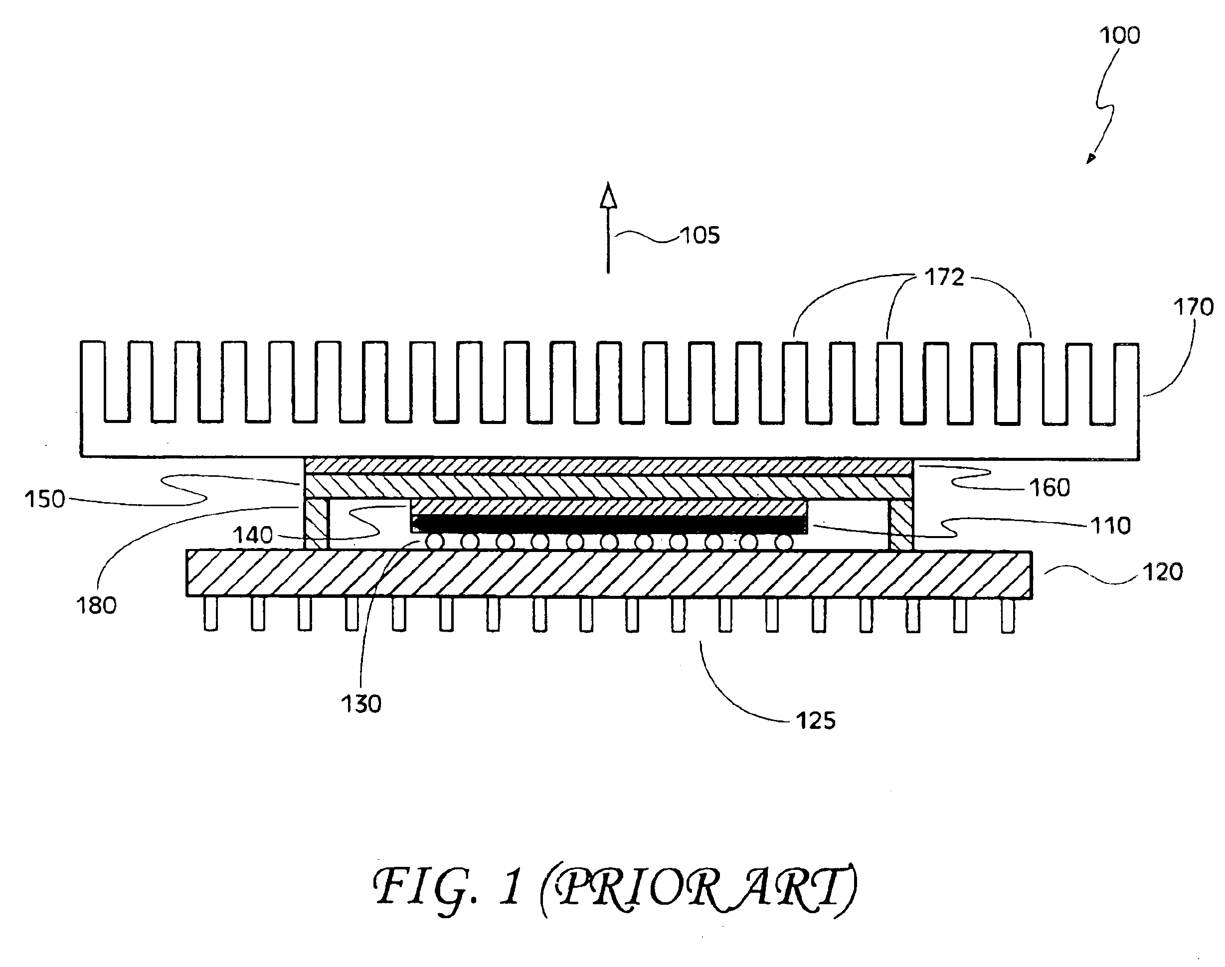
[0016]One possible solution to meet the heat dissipation needs of microprocessors and other processing devices is to employ a liquid cooling system—e.g., an active cooling system—rather than (or in combination with) heat sinks and other passive heat removal components. Disclosed herein are embodiments of a method for forming channels on a die, heat spreader, or other substrate, as well as embodiments of a liquid cooling system employing these channels for fluid flow.

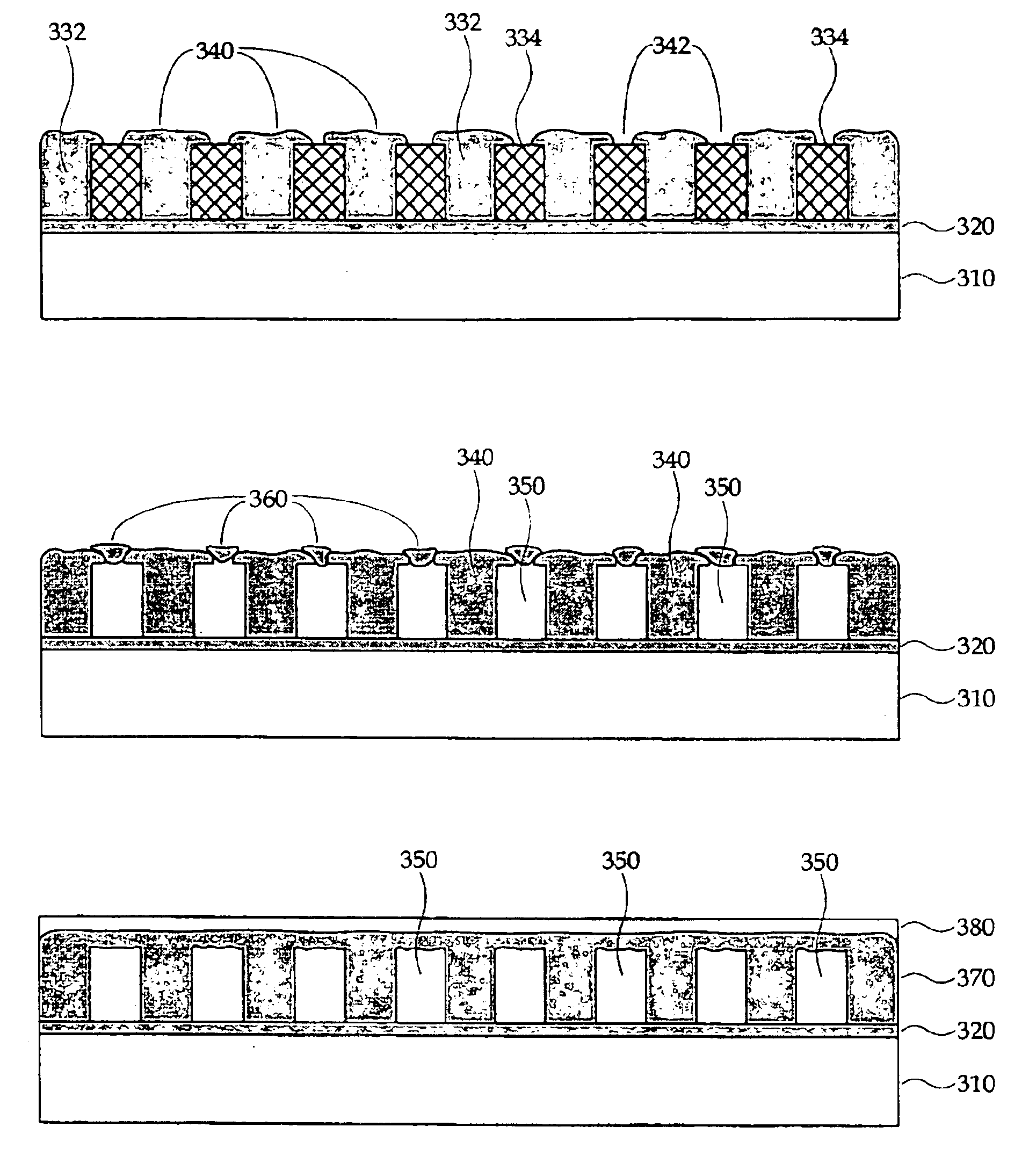
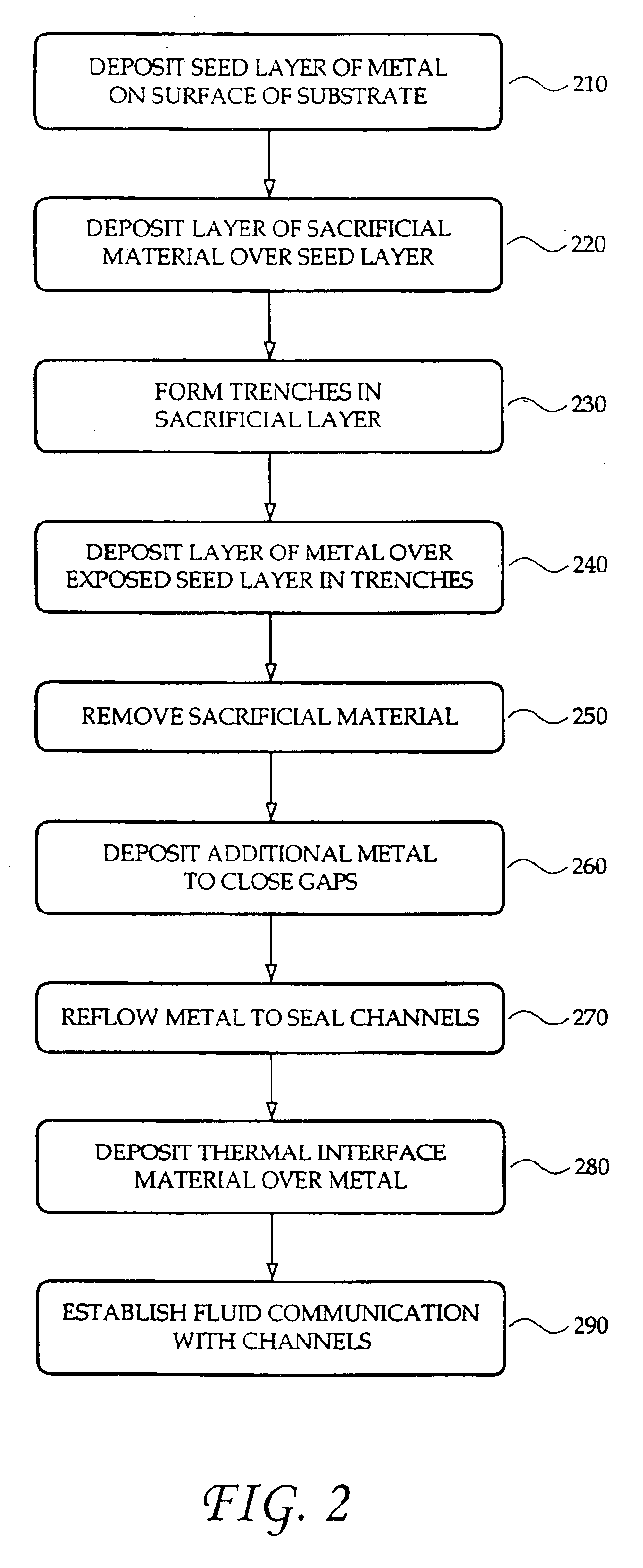
[0017]Illustrated in FIG. 2 are embodiments of a method for forming channels on a die, heat spreader, or other substrate. The method of FIG. 2 is further illustrated in the schematic diagrams provided in FIGS. 3A through 3H, and reference should be made to these figures as called out in the text below.

[0018]Referring now to FIG. 2, a seed layer of a metal is deposited on a surface of a substrate, as set forth in block 210. This is illustrated in FIG. 3A, which shows a substrate 310, and a seed layer 320 of a metal has be...


PUM


Abstract

A method of forming channels on a die or other substrate. Also disclosed are liquid cooling systems including such channels.

Description

FIELD OF THE INVENTION[0001]The invention relates generally to the packaging of an integrated circuit die and, more particularly, to methods of forming channels on a die or other substrate, as well as die cooling systems including such channels.BACKGROUND OF THE INVENTION[0002]Illustrated in FIG. 1 is a conventional packaged integrated circuit (IC) device 100. The IC device 100 includes a die 110 that is disposed on a substrate 120, this substrate often referred to as the “package substrate.” The die 110 may comprise a microprocessor, a network processor, or other processing device. Die 110 may be coupled with the substrate using, for example, a Controlled Collapse Chip Connection (or “C4”) assembly technique, wherein a plurality of leads, or bond pads, on the die 110 are electrically connected to a corresponding plurality of leads, or lands, on the substrate 120 by an array of connection elements 130 (e.g., solder bumps, columns, etc.). Circuitry on the package substrate 120, in tu...

Claims


Application Information

Patent Timeline
Patent Type & Authority Patents(United States)
IPC IPC(8): H01L21/48H01L21/68H01L23/473H01L21/02H01L21/67H01L23/34
CPCH01L23/473H01L2224/16H01L2224/73253H01L2924/01078H01L2924/15153H01L2924/15165H01L2924/15312H01L2924/16195
Inventor RAMANATHAN, SHRIRAMCHENG, CHIN CHANGMYERS, ALAN M.
Owner INTEL CORP
Why Eureka
Try Eureka