Electrical assembly and method for manufacturing the electrical assembly

a technology of electrical assembly and manufacturing method, which is applied in the direction of hermetically sealed casings, non-metallic protective coating applications, coupling device connections, etc., can solve the problems of various failure mechanisms, mechanical splitting and breakage of bonding wires, and the function failure of modules, etc., to prevent resonance vibration, prevent moisture damage, and manufacture with only a slight additional manufacturing expense

Inactive Publication Date: 2005-07-19
ROBERT BOSCH GMBH
View PDF10 Cites 2 Cited by
  • Summary
  • Abstract
  • Description
  • Claims
  • Application Information

AI Technical Summary

Benefits of technology

[0002]The electrical assembly according to the present invention, and the method according to the present invention for manufacturing an electrical assembly, have the advantage that a protective layer can be provided that is optimized with respect to mechanical and thermal loading capacity. No constructive measures are required at the electrical assembly itself, and no additional mechanical parts are required in order to fix the various regions in relation to one another or in order to prevent resonance vibrations of the material of the protective layer. On the one hand, the assembly is fail-safe even under extreme demands with respect to vibrational stress and temperature, while on the other hand it is well-protected against moisture, and in addition can be manufactured with only a slight additional manufacturing expense.
[0003]It is particularly advantageous to manufacture first regions, which surround elements that are mechanically sensitive and / or sensitive to corrosion, from a soft material, so that these elements are protected against moisture without being damaged mechanically when there are changes in temperature, because the soft gel can flow sufficiently around the bonding wires, while hard second regions, situated in complementary fashion hereto, protect the overall protective layer against damaging resonance vibrations and bonding damages potentially resulting therefrom. In the case of coverage of the first regions by the second regions, the first regions are additionally protected against the effects of moisture.
[0004]The use of gel materials has the advantage that these materials can economically be hardened at the same time, in a single baking process.
[0005]A simple limitation between the first and second regions can advantageously take place through the use of a thixotropic gel, i.e., a gel that is relatively fluid when in motion (when being poured in), and which, as soon as it comes to rest, enters into a gel-type state (thixotropy=reversible conversion between colloidal solution and gel). This thixotropic gel type that is first brought in can easily be brought into the desired regions, for example using a movable dispensing device that can be flexibly adjusted. In this way, the desired localization of the various gel types can be achieved without an additional constructive expense, and both gel regions can be hardened in a common baking step, without mixing of the two regions.

Problems solved by technology

Under certain conditions of use of the electronic module, damages of the bonding wires up to complete breakages of the wires, caused by mechanical action of the gel on the bonding wires, can occur during the life of the module, resulting in functional failure of the module.
According to the selected degree of hardness of the gel, various failure mechanisms can occur in this context.
The resulting cyclical motion of the bonding wires then finally leads to a mechanical splitting and breakage of the bonding wires.
If changes of temperature occur at the module, this has the result that the gel must move around the bonding wires in a flowing motion, because these wires cannot be deformed as strongly as would be necessary in order to be able to follow the thermally caused gel motion.
If the hardness of the gel is too great, these flowing motions can then likewise exert mechanical forces on the bonding wires that are so strong that these wires finally break, given sufficiently strong and frequent changes of temperature.

Method used


Image

  • Electrical assembly and method for manufacturing the electrical assembly
  • Electrical assembly and method for manufacturing the electrical assembly

Examples


Embodiment Construction

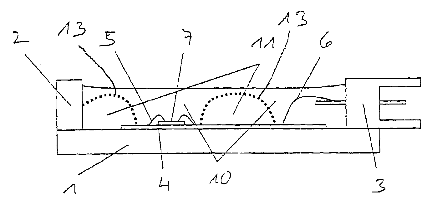
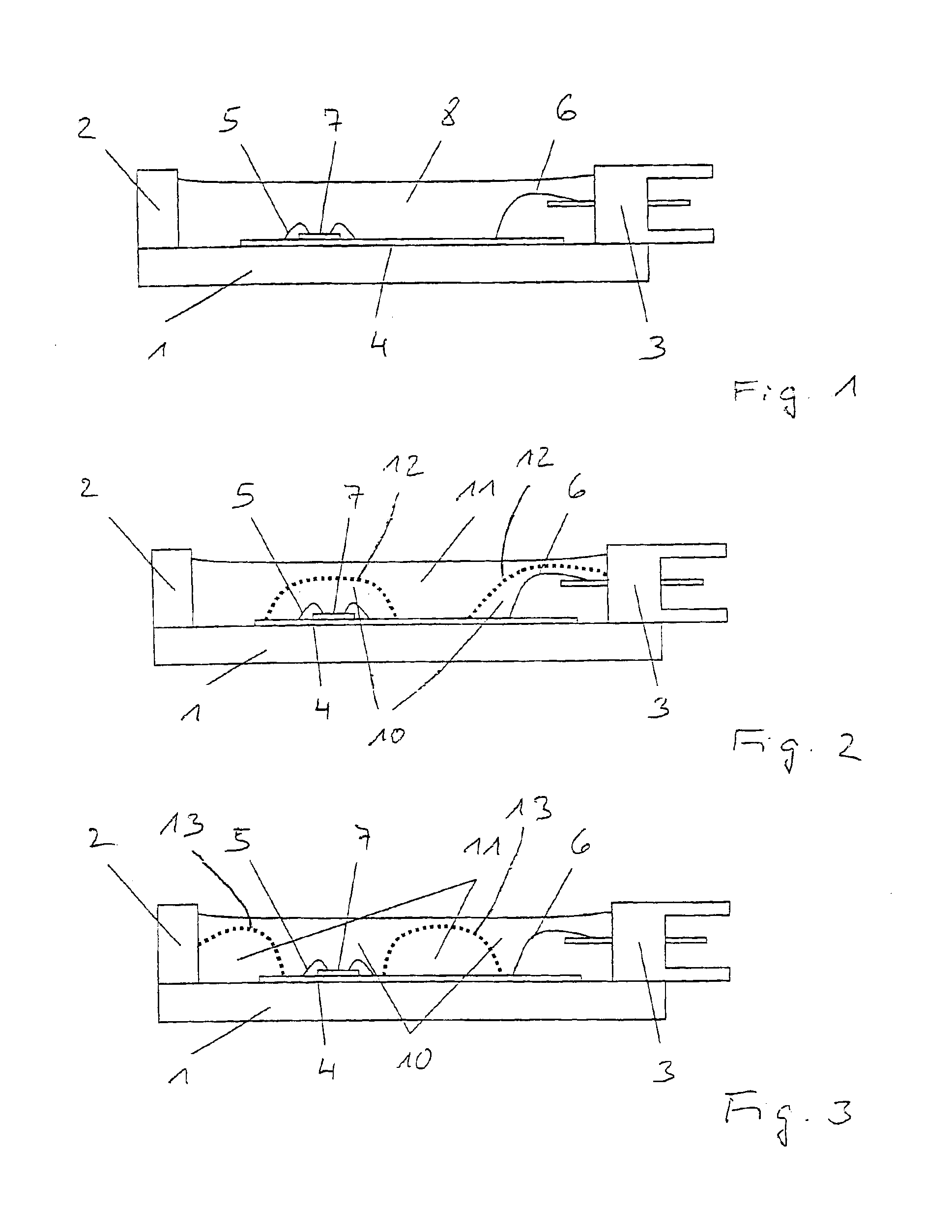
[0010]FIG. 1 shows a cross-sectional side view of an electrical assembly known from the prior art. Base plate 1 of the housing is surrounded by a frame 2 having a male connector 3 on one side. This male connector 3 is used for the contacting of an electronic circuit 4 that is connected with the male connector via thick wire bonds 6 (in the drawing, only one such wired connection 6 is shown). On electronic circuit 4 there is situated an unhoused semiconductor chip 7 that is connected electrically with the circuit via thin wire bonds 5. The housing is filled with silicon gel 8 to such an extent that all bonding wires are insulated from the surrounding air.

[0011]The filling with silicon gel protects the electronic circuit in order to protect unhoused chips and bonding wires from the effect of moisture; here it is necessary to cover the components to be protected with gel completely in order to ensure a sufficient protection against moisture. As an additional component of the module, a ...


PUM


Abstract

An electrical assembly including an electrical circuit situated in a housing, and a method for the manufacture of such an assembly, in which the electrical circuit is covered at least partially with a protective layer, wherein the protective layer has first and second regions having different hardnesses, so that the protective layer can be optimized with respect to mechanical and thermal loading capacity.

Description

BACKGROUND INFORMATION[0001]From German Patent Application No. 19722355.9, it is known to use a silicon gel as a covering layer in order to protect the electronic circuit. Under certain conditions of use of the electronic module, damages of the bonding wires up to complete breakages of the wires, caused by mechanical action of the gel on the bonding wires, can occur during the life of the module, resulting in functional failure of the module. According to the selected degree of hardness of the gel, various failure mechanisms can occur in this context. If the gel is too soft, and there are vibrational stresses on the module, as can occur for example in the case of an aggregate construction, then the gel compound, which may not be selected arbitrarily low in hardness due to the requirement of a complete covering of the components to be protected, can be excited to strong resonance vibrations that are in turn transmitted to the bonding wires. The resulting cyclical motion of the bondin...

Claims


Application Information

Patent Timeline
Patent Type & Authority Patents(United States)
IPC IPC(8): H01L23/28H01L23/31H01L23/16H01L23/24H05K3/28H01L23/29
CPCH01L23/24H01L23/3135H05K3/284H01L2224/48227H01L24/48H01L2224/05599H01L2224/45099H01L2224/85399H01L2924/00014H01L2924/181H01L2924/19107H01L2924/00012H01L2224/45015H01L2924/207
Inventor TOPP, RAINERTELLO, LAURA REYESBARTELS, ARNE
Owner ROBERT BOSCH GMBH
Why Eureka
Try Eureka