Method and system for measuring neutron emissions and ionizing radiation, solid state detector for use therein, and imaging system and array of such detectors for use therein

a technology for which is applied in the field of methods and systems for measuring neutron emission and ionizing radiation, solid state imaging systems and arrays of such detectors for use therein, and can solve the problems of not having all of the listed ideal material properties, large fraction, and required properties

Inactive Publication Date: 2005-07-26
RGT UNIV OF MICHIGAN
View PDF11 Cites 13 Cited by
  • Summary
  • Abstract
  • Description
  • Claims
  • Application Information

AI Technical Summary

Benefits of technology

[0017]In further carrying out the above object and other objects of the present invention, an imaging system for imaging neutron emissions and ionizing radiation is provided. The system includes an array of solid state detectors. Each of the detectors includes a first semiconductor active region for generating neutron-induced ionizing radiation in response to the neutron emissions and for generating a first electronic signal in response to the neutron emissions and ionizing radiation. Each of the detectors also includes a second semiconductor active region being substantially unresponsive to the neutron emissions for generating a second electronic signal in response to the ionizing radiation and a shield positioned to shield the neutron-induced ionizing radiation from the second semiconductor active region so that the second electronic signal is not generated in response to the neutron-induced ionizing radiation. The system further includes an array of sheets of high-density material for separating adjacent solid state detectors.

Problems solved by technology

Presently, no semiconductor has all of the listed ideal material properties desired for the “perfect” room temperature-operated, semiconductor radiation spectrometer, although many have a considerable fraction, of the required properties.
Unfortunately, a gamma ray field accompanies most neutron measurements.
Since the described devices are gamma ray detectors, confusion can arise regarding the difference between neutron-induced gamma rays and background gamma rays.
A method is described in the literature that allows for gamma ray discrimination, yet it has problems.
The method demonstrated that HgI2 with natural Hg could be used for a detector, however the accuracy of the measurement is questionable.
Hence, using lead as a shield reduces the device sensitivity to neutrons.
As a result, the actual gamma ray background is different for both devices and the subtracted spectrum produces an erroneous lower number of a neutron count.
Then, Cd sheet can be placed far away from the device (2.5 meters in the literature) to reduce the gamma ray background generated by the 113Cd(n,γ)114Cd reaction, yet the arrangement does not allow for the realization of a compact detecting instrument.

Method used


Image

  • Method and system for measuring neutron emissions and ionizing radiation, solid state detector for use therein, and imaging system and array of such detectors for use therein
  • Method and system for measuring neutron emissions and ionizing radiation, solid state detector for use therein, and imaging system and array of such detectors for use therein
  • Method and system for measuring neutron emissions and ionizing radiation, solid state detector for use therein, and imaging system and array of such detectors for use therein

Examples


Embodiment Construction

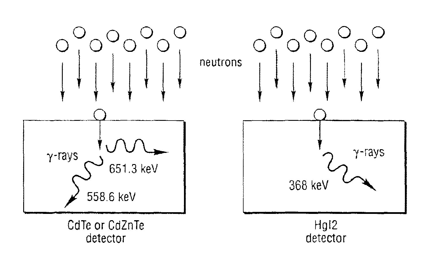
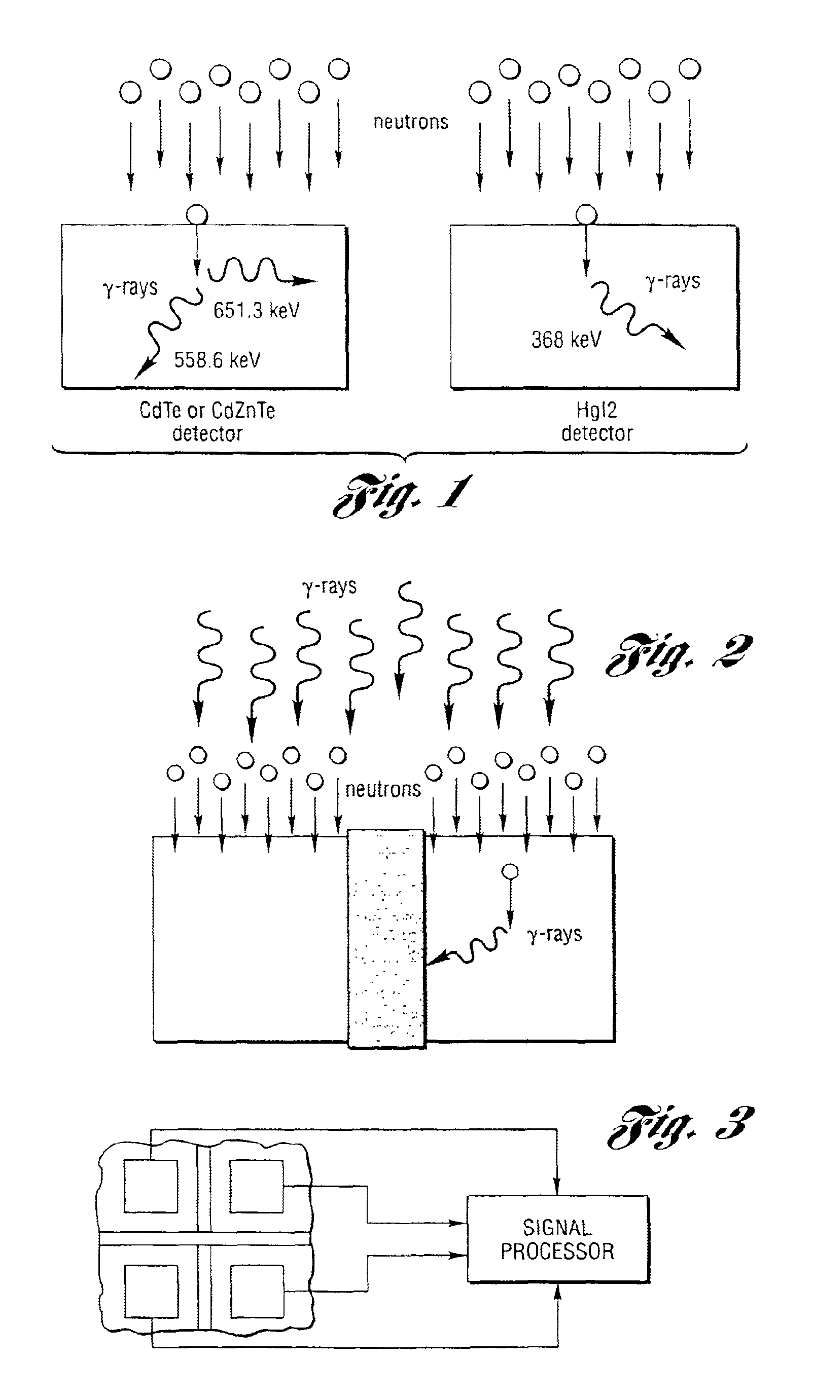
[0032]The present invention includes a radiation detector for neutron detection and discrimination. The detector is capable of measuring both neutrons and ionizing radiation such as gamma rays. The detector may be a portable, room temperature-operated, gamma ray spectrometer and neutron counter. Such a detector is capable of discriminating between background gamma ray events and neutron-induced events.

[0033]The detector preferably uses Cd- and / or Hg-containing semiconductor devices. The detector may use:

[0034]1. Natural concentrations of 113Cd or 199Hg;

[0035]2. Depleted and enriched concentrations of 113Cd or 199Hg;

[0036]3. Electronics capable of subtracting detector signals of one semiconductor device from another; and

[0037]4. A gamma ray shield between the devices.

[0038]The starting materials needed to grow HgI2, CdTe and CdZnTe can be depleted or enriched to either reduce or enhance neutron absorption. For instance, enriching the 199Hg in HgI2 from 16.9% up to 90% will allow for ...


PUM


Abstract

A method and system for measuring neutron emissions and ionizing radiation, such as gamma emissions, solid state detector for use therein, and imaging system and array of such detectors for use therein are provided using Cd- and/or Hg-containing semiconductors or B-based, Li-based or Gd-based semiconductors. The resulting systems and detectors used therein may be not only compact and portable, but also capable of operating at room temperature. The detectors may also be operable as gamma ray spectrometers.

Description

BACKGROUND OF THE INVENTION[0001]1. Field of the Invention[0002]This invention relates to methods and systems for measuring neutron emissions and ionizing radiation, solid state detectors for use therein, and imaging systems and arrays of such detectors for use therein.[0003]2. Background Art[0004]The material requirements for a room temperature-operated, high resolution semiconductor gamma ray spectrometer include large free charge carrier mobilities (μ), or alternatively, high achievable free charge carrier velocities (ν), long mean free drift times (τ*), a relatively large energy band gap (Eg), generally between 1.4 eV to 2.5 eV, high representative values of atomic number (Z), and availability in large volumes. Presently, no semiconductor has all of the listed ideal material properties desired for the “perfect” room temperature-operated, semiconductor radiation spectrometer, although many have a considerable fraction, of the required properties. Some wide band gap compound semic...

Claims


Application Information

Patent Timeline
Patent Type & Authority Patents(United States)
IPC IPC(8): G01T3/00G01T3/08
CPCG01T3/08
Inventor MCGREGOR, DOUGLAS S.
Owner RGT UNIV OF MICHIGAN
Why Eureka
Try Eureka