Semiconductor process and composition for forming a barrier material overlying copper

a technology of copper and barrier material, applied in the field of formation, can solve the problems of reducing the chemical stability of electroless plating baths

Inactive Publication Date: 2005-08-02
APPLE INC
View PDF8 Cites 42 Cited by
  • Summary
  • Abstract
  • Description
  • Claims
  • Application Information

AI Technical Summary

Problems solved by technology

Many barrier formation techniques require catalytic activation which often has problems of selectivity due to a high probability of nucleation in non-metal area.
Non-activation barrier deposition processes typically require operating temperatures which are relatively higher for conventional electroless methods, and such higher temperatures reduce the chemical stability of electroless plating baths.

Method used


Image

  • Semiconductor process and composition for forming a barrier material overlying copper
  • Semiconductor process and composition for forming a barrier material overlying copper

Examples


Embodiment Construction

)

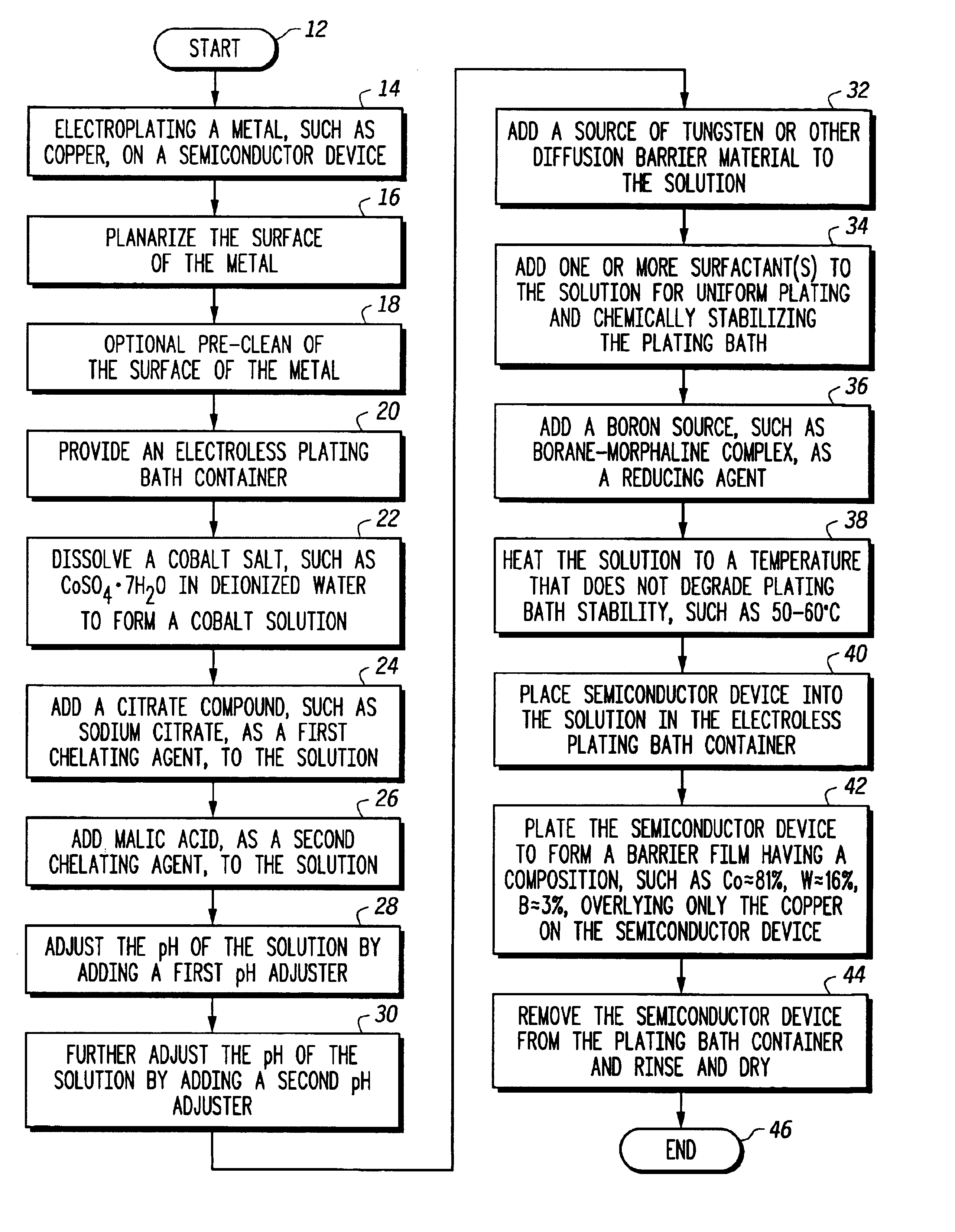
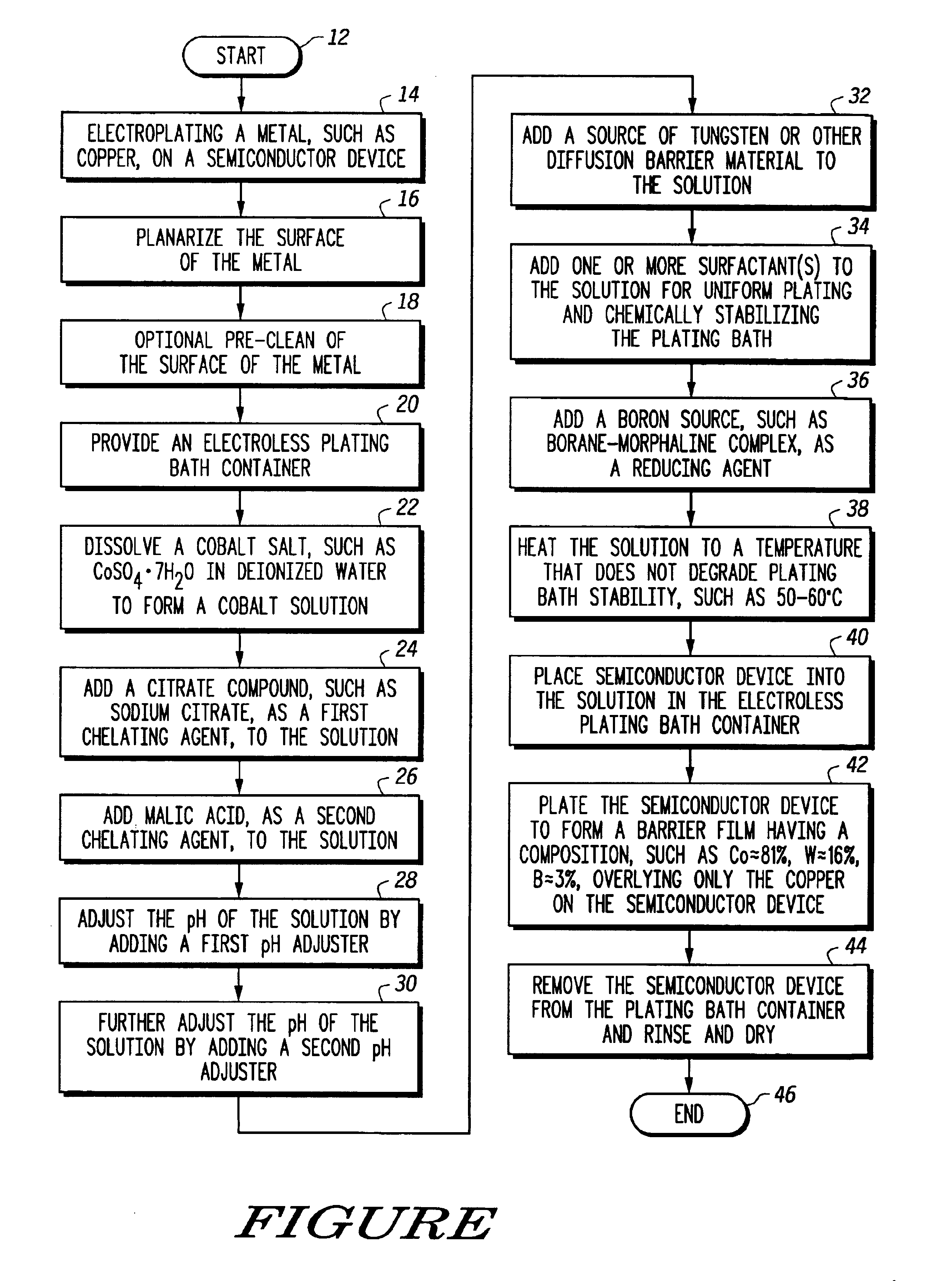
[0009]The following discussion is intended to provide a detailed description of at least one example of the invention and should not be taken to be limiting of the invention itself. Rather, any number of variations may fall within the scope of the invention which is properly defined in the claims following this description.

[0010]In one embodiment, a method for forming an integrated circuit is provided. The integrated circuit uses a copper interconnect structure which includes copper contacts in a first metal layer coupled to copper contacts in a second metal layer. The copper contacts are coupled in accordance with the circuit design by copper vias providing an electrical coupling therebetween. The integrated circuit also includes a dielectric material such as silicon dioxide or a low-k material disposed around the copper contacts and vias. To prevent diffusion of copper from the contacts and vias, a barrier material is formed between the low k material and the contacts and vias.

[0...


PUM

PropertyMeasurementUnit
temperatureaaaaaaaaaa
concentrationsaaaaaaaaaa

Abstract

An electroless plating process for forming a barrier film such as a cobalt tungsten boron film on copper interconnects lines of semiconductor wafers uses a plating bath of morpholine borane which provides higher thermal stability and range, allowing for greater compatibility with low k dielectric materials. Mixed chelating agents with different stability constants with a metal source are used to complex base metal such as copper which dissolves into solution, if any. A fluorosurfactant is used as a wetting agent and stabilizer.

Description

BACKGROUND[0001]1. Field[0002]The present invention relates to formation (e.g., deposition) of films in devices such as semiconductor and integrated circuit devices, and, more particularly, to diffusion barrier films in semiconductor devices.[0003]2. Description of the Related Art[0004]The semiconductor industry is constantly searching for ways to increase the speed of integrated circuits. For example, faster interconnect technology such as copper interconnects provide an improvement over older technologies since copper provides a faster signal medium.[0005]In integrated circuits, a dielectric layer is used to provide insulation around the interconnect wiring of the chip. Just as faster interconnect materials such as copper allow a signal to move faster through the chip, decreasing the capacitance factor of the insulating material also allows signals to travel across the interconnect faster because they have less interference with each other. The most common dielectric material is s...

Claims


Application Information

Patent Timeline
Patent Type & Authority Patents(United States)
IPC IPC(8): H01L21/70H01L21/288H01L21/768H01L21/02C23C18/34H01L23/532
CPCH01L21/288H01L21/76849H01L23/53238H01L2924/0002H01L2924/00
Inventor MATHEW, VARUGHESEGARCIA, SAM S.PRINDLE, CHRISTOPHER M.
Owner APPLE INC
Why Eureka
Try Eureka