Post ECP multi-step anneal/H2 treatment to reduce film impurity

a multi-step anneal/h2 treatment and film impurity technology, applied in the field of metal interconnects, can solve the problems of reduced performance, carbon may become trapped within the deposited metal layer, and the copper interconnect is facing the increasingly difficult challenge of forming a copper interconnect without voids, etc., to achieve low impurity concentration, improve reliability, and reduce the effect of defect density

Inactive Publication Date: 2005-10-13
TAIWAN SEMICON MFG CO LTD
View PDF8 Cites 56 Cited by
  • Summary
  • Abstract
  • Description
  • Claims
  • Application Information

AI Technical Summary

Benefits of technology

[0015] An objective of the present invention is to provide a metal interconnect with a low...

Problems solved by technology

As the widths of vias and trenches shrink, the semiconductor industry is faced with the increasingly difficult challenge of forming a copper interconnect without voids.
Voids can easily form along grain boundaries during metal deposition and cause reliability issues.
Small amounts of these ions are frequently trapped inside the deposited copper layer and the resulting sulfate and chloride impurity can lead to corrosion and reduced performance.
Furthermore, organic additives containing carbon are frequently used in the electrolyte solution and carbon may become trapped within the deposited metal layer.
Referring to FIG. 2, a portion of the copper layer 8 in FIG. 1 is shown which has a grain boundary 8a. A void defect 9 is shown along the grain boundary 8a. Unfortunately, in a prior art process where only one anneal is performed after the copper layer 8 is deposited, there is an unacceptably large number of void defects formed in...

Method used


Image

  • Post ECP multi-step anneal/H2 treatment to reduce film impurity
  • Post ECP multi-step anneal/H2 treatment to reduce film impurity
  • Post ECP multi-step anneal/H2 treatment to reduce film impurity

Examples


first embodiment

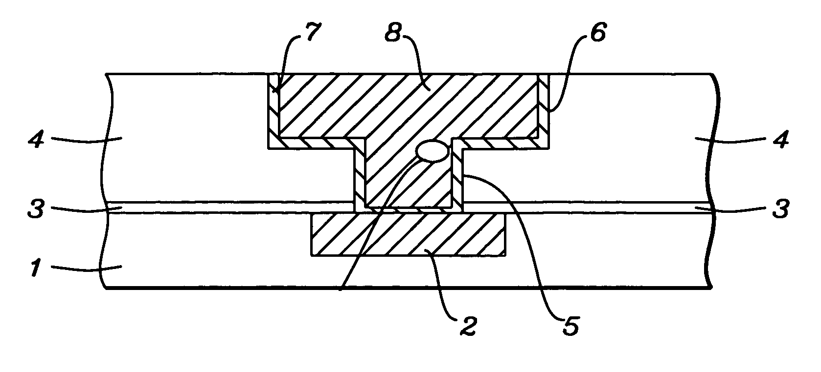
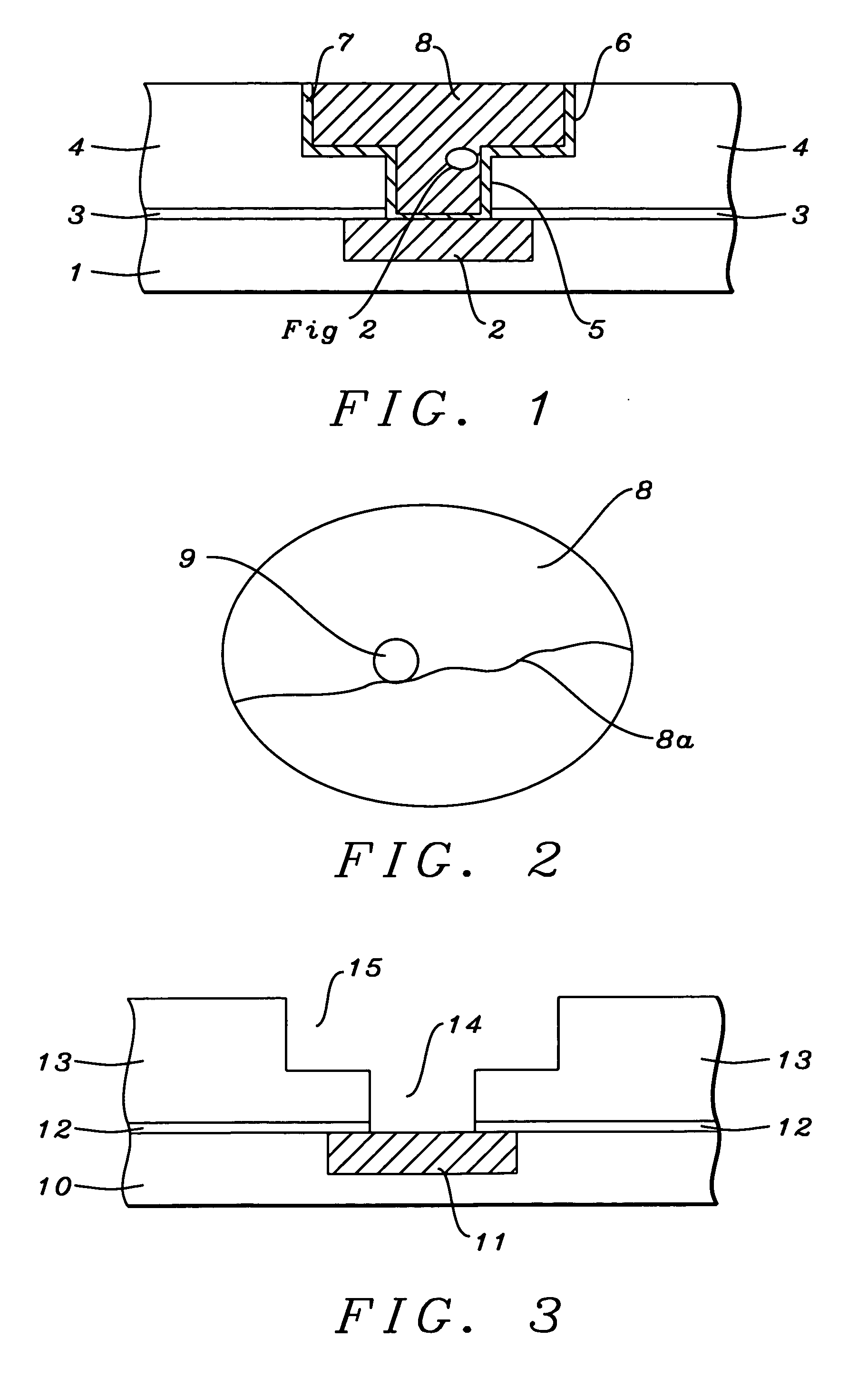
[0034] the present invention is illustrated in FIGS. 3-7 with regard to the formation of an interconnect in a dual damascene scheme. However, the method may also be applied to forming an interconnect in single damascene structure such as a trench. Referring to FIG. 3, a substrate 10 is provided that is typically silicon and may include active and passive devices that are not shown in order to simplify the drawing. A conductive layer 11 is formed in substrate 10 by conventional means and is comprised of a metal such as Al, Cu, W, or an Al / Cu alloy. Optionally, the conductive layer 11 is formed on a diffusion barrier layer (not shown) within substrate 10. A diffusion barrier layer is used to protect the conductive layer from trace amounts of impurities in substrate 10 that may cause corrosion or oxidation of the conductive layer 11. A diffusion barrier layer will also prevent metal ions in the conductive layer 11 from diffusing into substrate 10 and diminishing the insulating capabili...

second embodiment

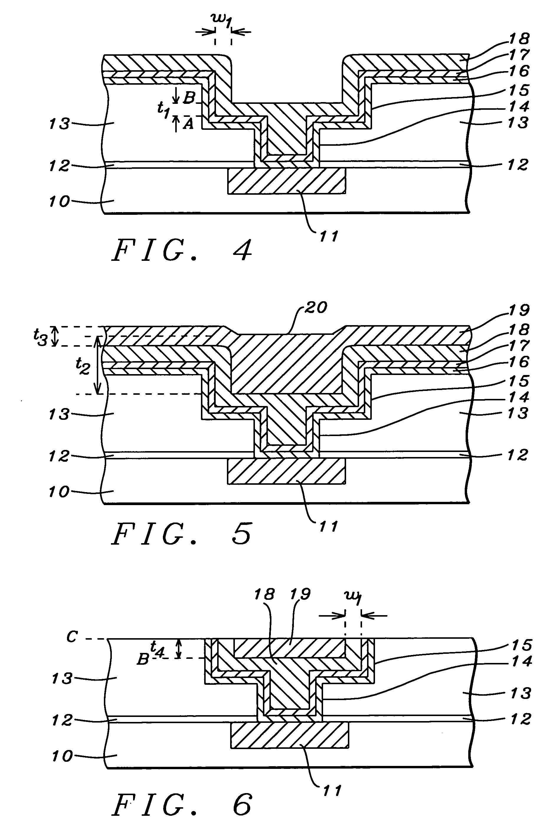
[0061] Referring to FIG. 9, the distance d between the top of the dielectric layer 13 and the surface 20 of the second metal layer 19 above the trench 15 may increase as a result of the second anneal. There may be a reflow of the second metal layer 19 that causes low portions on the surface 20 to become slightly elevated while some of the higher portions on the surface are lowered. The surface of the second metal layer is still uneven after the second anneal. Next, a third metal layer 21 is preferably deposited as an overfill of the trench 15 so that a subsequent planarization process does not cause a divot or dishing defect in the second metal layer 19 within the trench. Although the second metal layer 19 could be formed at a larger thickness to avoid the need for a third metal deposition, the second anneal of a thick second metal layer would not be as effective in removing impurities as from a thinner second metal layer 19 according to the

[0062] Therefore, a third ECP process is p...


PUM


Abstract

A method of forming a copper interconnect in a dual damascene scheme is described. After a diffusion barrier layer and seed layer are sequentially formed on the sidewalls and bottoms of a trench and via in a dielectric layer, a first copper layer is deposited by a first ECP process at a 10 mA/cm2 current density to fill the via and part of the trench. A first anneal step is performed to remove carbon impurities and optionally includes a H2 plasma treatment. A second ECP process with a first deposition step at a 40 mA/cm2 current density and second deposition step at a 60 mA/cm2 current density is used to deposit a second copper layer-that overfills the trench. After a second anneal step, a CMP process planarizes the copper layers. Fewer copper defects, reduced S, Cl, and C impurities, and improved Rc performance are achieved by this method.

Description

RELATED PATENT APPLICATION [0001] This application is related to the following: Docket # TS03-346, Ser. No. ______, filing date ______; assigned to a common assignee.FIELD OF THE INVENTION [0002] The invention relates to a metal interconnect with a low impurity content and a method for making the same that involves a damascene method in which an opening is filled in two metal deposition steps with an anneal after each step. BACKGROUND OF THE INVENTION [0003] Integrated circuits in a semiconductor device are comprised of metal wiring that is insulated by a dielectric layer to prevent capacitance coupling or crosstalk between the electrical pathways. Metal wiring that forms interlevel and intralevel connections which are commonly referred to as interconnects is frequently formed by depositing a metal in an opening such as a via hole or a trench in a single damascene approach or in a trench and via simultaneously in a dual damascene scheme. Usually, a diffusion barrier layer is formed ...

Claims


Application Information

Patent Timeline
IPC IPC(8): H01L21/311H01L21/768
CPCH01L21/2885H01L21/76877
Inventor FENG, HSIEN-PINGTSAO, JUNG-CHIHCHENG, HSI-KUEILEE, CHIH-TSUNGCHENG, MING-YUANLIN, STEVENCHUANG, RAYLIU, CHI-WEN
Owner TAIWAN SEMICON MFG CO LTD
Why Eureka
Try Eureka