Two step copper electroplating process with anneal for uniform across wafer deposition and void free filling on ruthenium coated wafers

a technology of ruthenium coating and copper electroplating, which is applied in the direction of electrolysis process, solid-state device, electrolysis components, etc., can solve the problems of difficult or impossible filling of features with electroplating process, less conformal film covering trench sidewalls and bottoms, and high cost of cvd methods compared to pvd processes. , to achieve the effect of reducing the likelihood of copper oxide formation

Active Publication Date: 2011-06-21
NOVELLUS SYSTEMS
View PDF76 Cites 54 Cited by
  • Summary
  • Abstract
  • Description
  • Claims
  • Application Information

AI Technical Summary

Benefits of technology

[0015]After the copper seed layer is deposited, the wafer may be stored or annealed. Under ambient conditions, a layer of copper oxide forms on copper seed layers. When exposed to the acidic environment in the bulk electroplating solution, the copper oxide dissolves into the electroplating solution. This dissolution is undesirable because it removes a portion of the copper seed layer that is required for bulk electroplating and may render the copper seed laye

Problems solved by technology

Chemical vapor deposition (CVD) methods can deposit a conformal copper seed layer with good adhesion, but CVD methods are expensive as compared to PVD processes.
Physical vapor deposition (PVD) methods can deposit a copper seed layer with good adhesion, but produces a less conformal film that covers the sidewalls and bottoms of trenches poorly.
The thicker PVD seed layer increases aspect ratios in features and may pinch off the gap opening, making the features harder or impossible to fill with an electroplating process.
As feature sizes decrease, the limitation

Method used


Image

  • Two step copper electroplating process with anneal for uniform across wafer deposition and void free filling on ruthenium coated wafers
  • Two step copper electroplating process with anneal for uniform across wafer deposition and void free filling on ruthenium coated wafers
  • Two step copper electroplating process with anneal for uniform across wafer deposition and void free filling on ruthenium coated wafers

Examples


Embodiment Construction

Introduction and Overview

[0024]In the following description, numerous specific details are set forth in order to provide a thorough understanding of the present invention. The present invention may be practiced without some or all of these specific details. In other instances, well known process operations have not been described in detail to not unnecessarily obscure the present invention. While the invention will be described in conjunction with the specific embodiments, it will be understood that it is not intended to limit the invention to the embodiments.

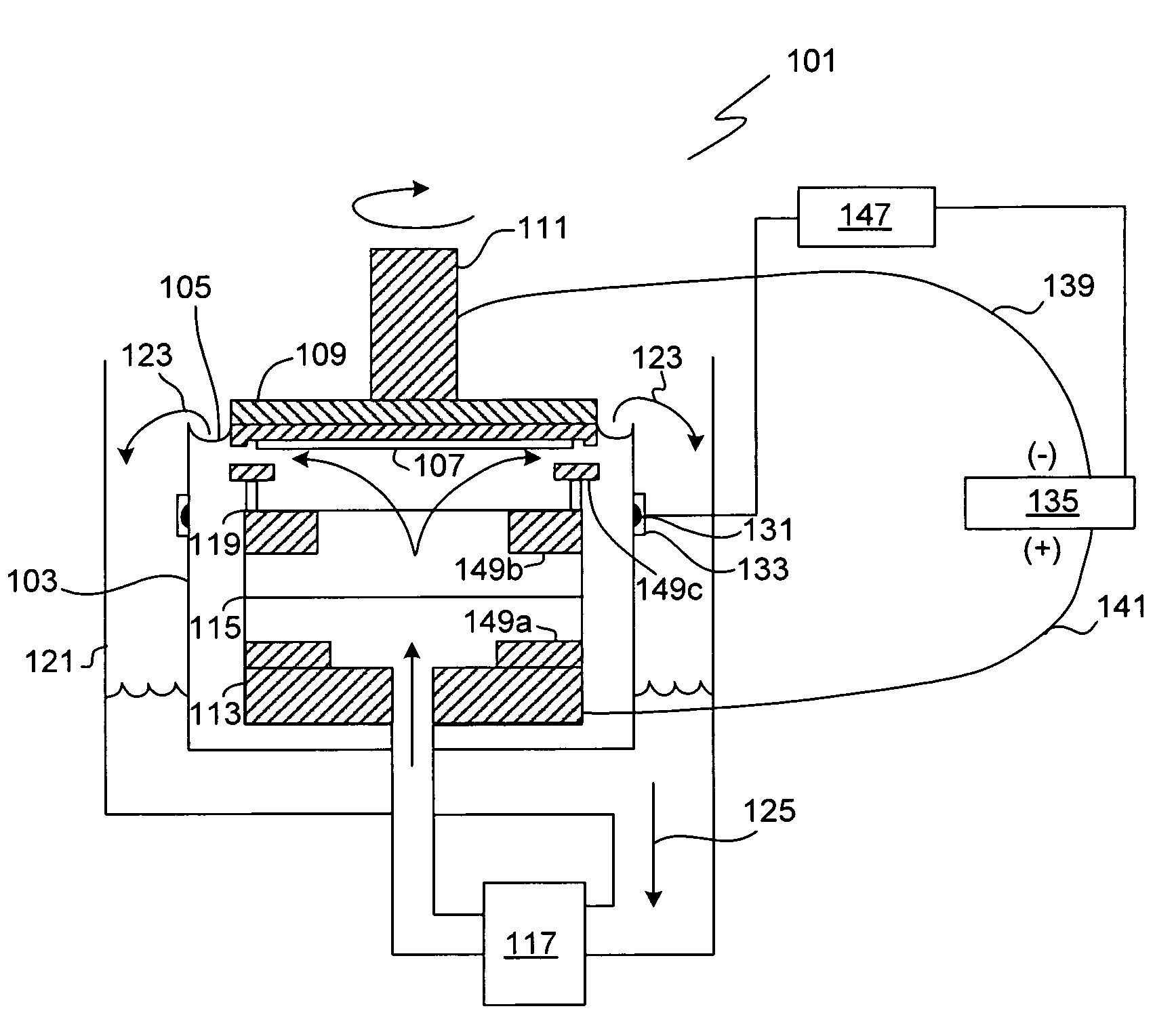
[0025]In this disclosure various terms are used to describe a semiconductor processing work surface, “wafer” and “substrate” are used interchangeably. The process of depositing, or plating, metal onto a conductive surface via an electrochemical reaction are referred to generally as electroplating or electrofilling. Bulk electrofilling refers to electroplating a relatively large amount of copper to fill trenches and vias.

[0026]A...


PUM

PropertyMeasurementUnit
Temperatureaaaaaaaaaa

Abstract

A two-step semiconductor electroplating process deposits copper onto wafers coated with a semi-noble metal in manner that is uniform across the wafer and free of voids after a post electrofill anneal. A seed-layer plating bath nucleates copper uniformly and conformably at a high density in a very thin film using a unique pulsed waveform. The wafer is then annealed before a second bath fills the features. The seed-layer anneal improves adhesion and stability of the semi-noble to copper interface, and the resulting copper interconnect stays void-free after a post electrofill anneal.

Description

FIELD OF THE INVENTION[0001]The present invention relates generally to methods and apparatus for depositing copper onto a wafer and more particularly to methods and apparatus for electroplating a copper seed layer on a semiconductor wafer. It is particularly useful for electroplating copper in damascene and dual damascene integrated circuit fabrication methods.BACKGROUND OF THE INVENTION[0002]Manufacturing of semiconductor devices commonly requires deposition of electrically conductive material on semiconductor wafers. The conductive material, such as copper, is often deposited by electroplating onto a seed layer of copper deposited onto the wafer surface by a PVD or CVD method. Electroplating is a method of choice for depositing metal into the vias and trenches of the processed wafer during damascene and dual damascene processing.[0003]Damascene processing is used for forming interconnections on integrated circuits (ICs). Damascene processing involves formation of inlaid metal line...

Claims


Application Information

Patent Timeline
IPC IPC(8): H01L21/44
CPCC25D3/38C25D5/18C25D5/50H01L21/2885H01L21/76864H01L21/76873C25D7/123H01L21/76843C25D17/001H01L2221/1089
Inventor PONNUSWAMY, THOMASSUKAMTO, JOHNREID, JONATHANMAYER, STEVE
Owner NOVELLUS SYSTEMS
Why Eureka
Try Eureka