Copper interconnect systems which use conductive, metal-based cap layers

a copper interconnect and metal-based cap technology, applied in the field of electromechanical devices, can solve the problems of inherently extremely difficult control of processes, degrade the electromigration resistance of the system, and none of the inventions disclose copper interconnect systems, so as to improve the resistance against electromigration (em), reduce the use of high dielectric insulators, and enhance the adhesion or interfacial bonding

Active Publication Date: 2006-04-11
INTELLECTUAL VENTURES ASSETS 185
View PDF15 Cites 54 Cited by
  • Summary
  • Abstract
  • Description
  • Claims
  • Application Information

AI Technical Summary

Benefits of technology

[0008]In view of the foregoing background, it is therefore an object of the present invention to provide a copper interconnect system which uses a conductive, metal-based cap layer, and substantially direct copper-to-copper contact at the interface of the copper via to the underlying copper interconnect. The invention, with its several embodiments, is focused on damascene type implementations. Within the dual-damascene structure, doped, that is, alloy seed layers may be used both against dielectric (insulating) and metal-based or con

Problems solved by technology

But none of these inventions discloses a copper interconnect system where a copper via to underlying copper interconnect makes a substantially direct copper to copper connection without the presence of an intervening diffusion barrier.
The presence of such a barrier tends to degrade the electromigration resistance of the system.
Such a process is inherently extremely difficult to control, the main problem residing in controlling the required wide variation in seed layer thicknesses.
Such a process is also inherently extremely difficult to control.
Neither of these prior art references discloses use of a metal-based cap layer, alloy seed layers, or methods o

Method used


Image

  • Copper interconnect systems which use conductive, metal-based cap layers
  • Copper interconnect systems which use conductive, metal-based cap layers
  • Copper interconnect systems which use conductive, metal-based cap layers

Examples


first embodiment

[0014]The following first embodiment is directed to improving the various weaknesses of prior art copper interconnect technology as discussed in detail above. These include weak bonding of the copper interconnect at the various interfaces present. Among various improvements, this invention teaches the use of certain metals and alloys to improve the bonding. This results in greatly reduced interface diffusion rates. This improves EM resistance, and reduces stress induced migration failure rates.

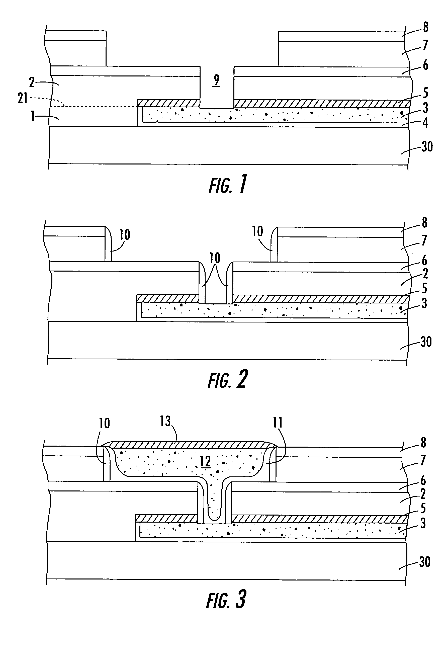
[0015]Referring to FIG. 1, a first Damascene-type interconnect comprising copper 3 is formed in an SiO2 or low-k type insulator 1 that, in turn, is on or adjacent a substrate 30. A liner 4 is formed by PVD, CVD or by (atomic layer deposition) ALD or by other methods, of Ta, Ta / TaN, Ta / TaN / Ta or other combinations thereof, or, for adhesion enhancement, an alloy or mixture comprising Ti added to Ta, Cr, Mo, W, Rh, Ru or Re—such alloys yielding improved adhesion to copper based metal 3. The barri...

second embodiment

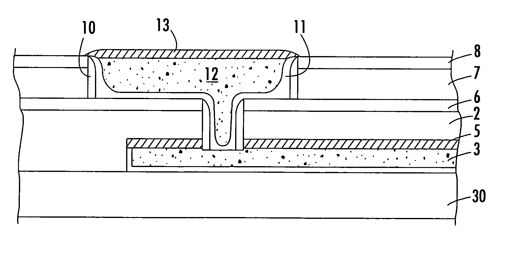
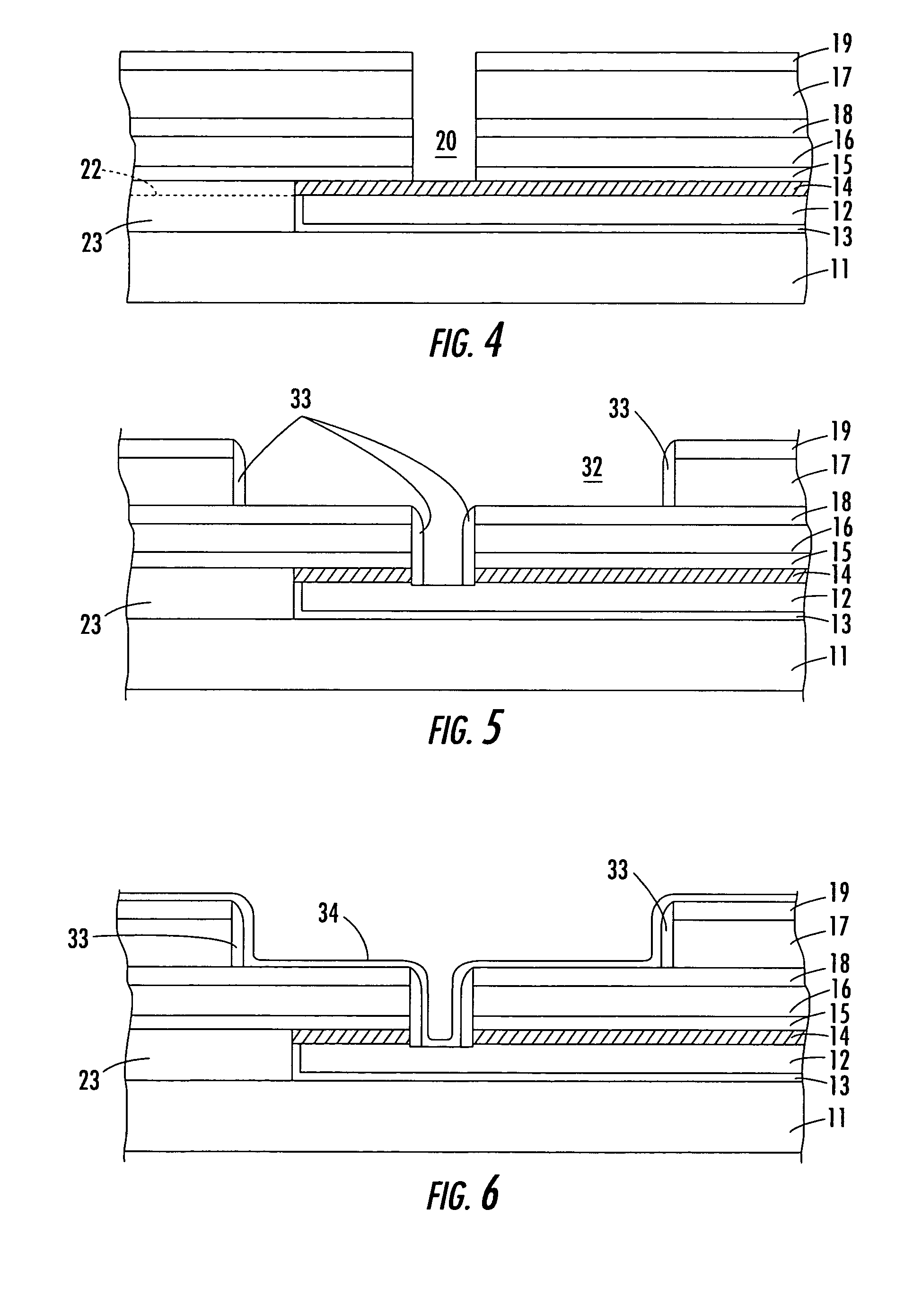
[0021]Referring now additionally to FIGS. 4–6, a second embodiment provides a conductive coating or cap layer on the copper interconnect surface for the purpose of interface diffusion rate reduction. The coating is not a robust diffusion barrier, and for that reason it is covered by a dielectric diffusion barrier. The coating is etchable in halide-containing anisotropic plasma etching chemistries (RIE), and may be removed so that overlying copper vias may make a more direct copper-to-copper connection. This aids the prevention of copper flux divergence at the base of a via, a phenomenon which tends to reduce EM resistance. This embodiment also has no substantial diffusion barrier thickness remaining at the base of copper vias.

[0022]Following FIG. 4, a copper based interconnect 12 is formed over substrate 11 by a damascene-type process. The trench is lined with diffusion barrier 13 as described in the first embodiment above. The film 23 below the dashed line 22 is an insulating layer...


PUM


Abstract

An integrated circuit (IC) may include a substrate, a first dielectric layer adjacent the substrate, and at least one trench in the first dielectric layer. The IC may also include a metal liner within the at least one trench, and a first conductive region including copper within the at least one trench. A cap layer including metal may be provided on the first conductive region. A second dielectric layer may be over the first conductive region and the cap layer. A dielectric etch stop and diffusion barrier layer may be over the second dielectric layer, and a via may be over the first conductive region and through the second dielectric layer and the cap layer. A diffusion barrier layer may be on sidewalls of the via, and an alloy seed layer including copper and at least one of tantalum, molybdenum, chromium, and tungsten may be over the diffusion barrier. The alloy seed layer may also be over the dielectric etch stop and diffusion barrier layer, and the alloy seed layer may be in contact with the first conductive region.

Description

RELATED APPLICATION[0001]This application is based upon prior filed provisional application Ser. No. 60 / 455,496 filed May 27, 2003, the entire subject matter of which is incorporated herein by reference in its entirety.FIELD OF THE INVENTION[0002]The present invention relates to the field of electronics, and, more particularly, to semiconductor devices including copper interconnects and related methods. Even more particularly, the invention relates to reliability improvements for copper interconnects.BACKGROUND OF THE INVENTION[0003]Doped seed layers have been disclosed in the prior art, their presence directed to various objectives. These include U.S. Pat. No. 5,969,422 to Ting et al.; U.S. Pat. No. 6,249,055 to Dubin; U.S. Pat. No. 6,181,012 to Edelstein et al.; U.S. Pat. No. 6,066,892 to Ding et al.; and U.S. Pat. No. 6,461,675 to Paranjpe et al. But none of these inventions discloses a copper interconnect system where a copper via to underlying copper interconnect makes a substa...

Claims


Application Information

Patent Timeline
IPC IPC(8): H01L23/52H01L21/768H01L23/532
CPCH01L21/76805H01L21/76807H01L21/76831H01L21/76843H01L21/76844H01L21/76849H01L23/53238H01L21/76858H01L21/76864H01L21/76865H01L21/76873H01L21/76886H01L21/76855H01L2924/0002H01L2924/00
Inventor CUNNINGHAM, JAMES A.
Owner INTELLECTUAL VENTURES ASSETS 185
Why Eureka
Try Eureka