Organic EL pixel circuit

Inactive Publication Date: 2005-08-02
SANYO ELECTRIC CO LTD
View PDF6 Cites 190 Cited by
  • Summary
  • Abstract
  • Description
  • Claims
  • Application Information

AI Technical Summary

Benefits of technology

[0011]The present invention was conceived in view of the aforementioned problems of the prior art and ai

Problems solved by technology

Accordingly, such a conventional pixel circuit has a problem that even when the TFT2 is off, a current flows in the organic EL element EL in accordance with the charges accumulated in the capacitor of the organic EL element, thereby generating an afterimage.
More specifical

Method used


Image

  • Organic EL pixel circuit
  • Organic EL pixel circuit
  • Organic EL pixel circuit

Examples


Embodiment Construction

[0028]Preferred embodiments of the present invention will be described in further detail with reference to the accompanying drawings.

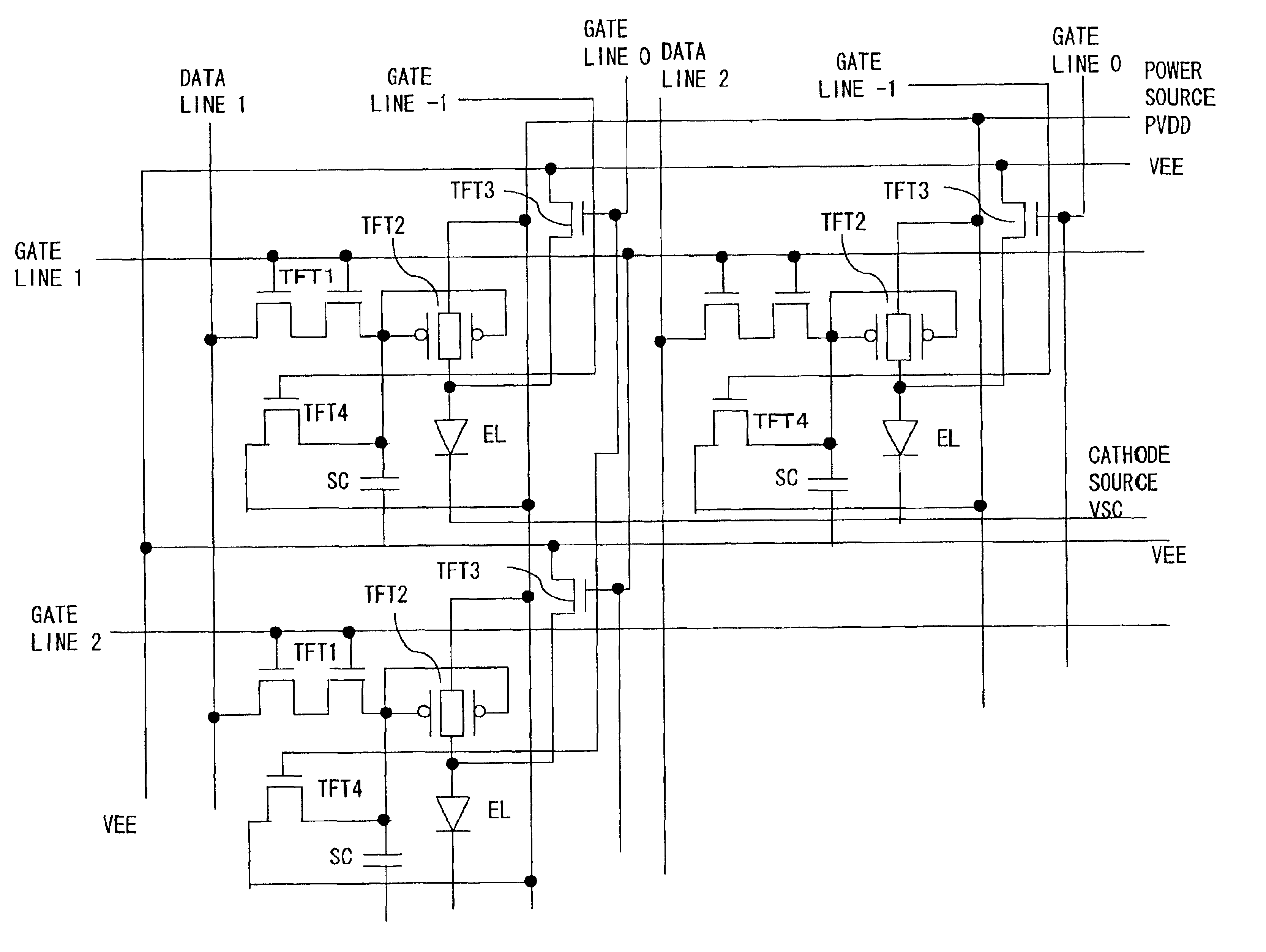
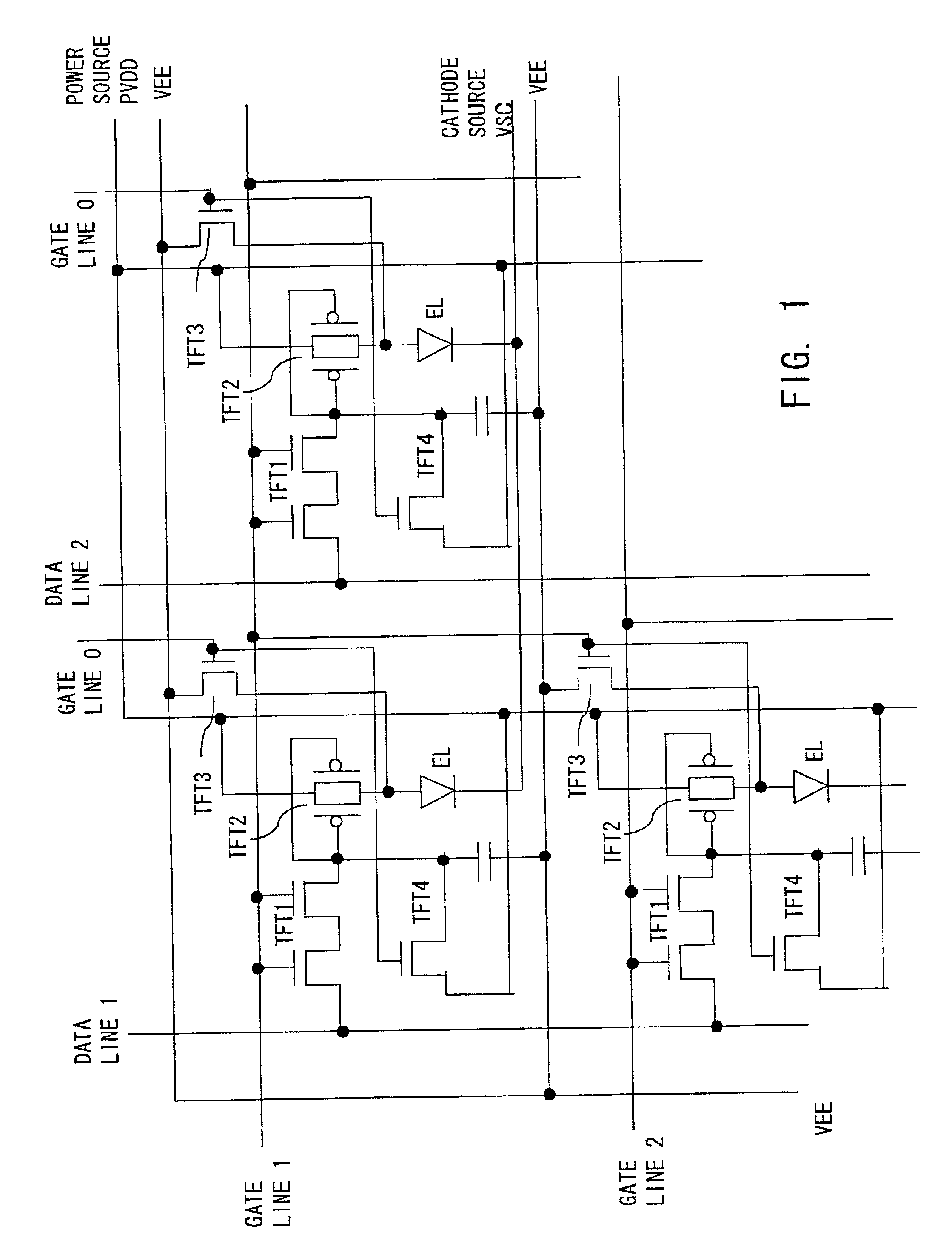
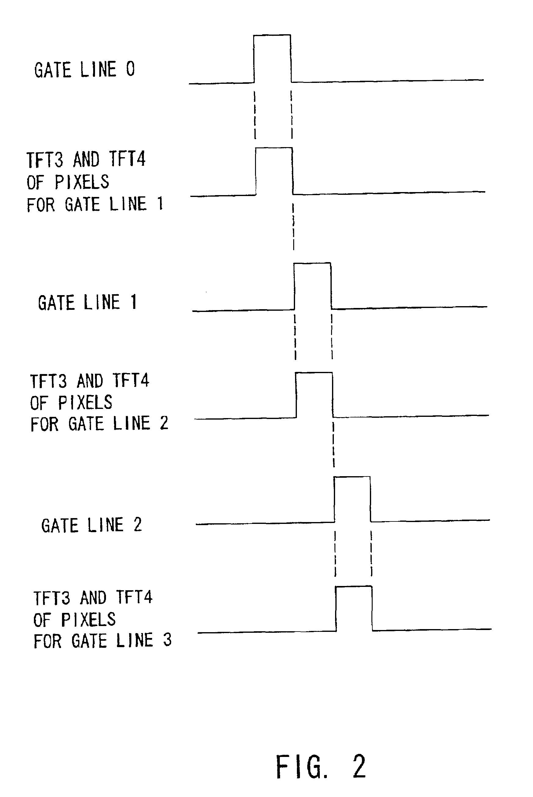
[0029]FIG. 1 illustrates a structure of a pixel circuit corresponding to one pixel portion according to one embodiment of the present invention. To a gate line extending in the horizontal direction, a TFT1 comprising a n-channel TFT is connected. The TFT1, which is formed as a double-gate type TFT having TFTs connected in series in this embodiment, need not necessarily be of the double-gate type.

[0030]The other end of the TFT1 is connected with one end of the storage capacitor SC. The other end of the storage capacitor SC is connected with VEE, which is a negative power source of the panel. To the node connecting the TFT1 and the storage capacitor SC, the gate of the drive transistor TFT2 comprising a p-channel TFT is connected. The TFT2, which is formed of two TFTs connected in parallel, has one end connected with the panel power source PVDD and the o...


PUM


Abstract

A discharge transistor (TFT3) which connects the upper end of an organic EL element (EL) and a negative power source (VEE) and a control transistor (TFT4) which connects the upper end of a storage capacitor (SC) with a power source (PVDD) are provided. These transistors (TFT3, TFT4) are turned on by the upper gate line, so that the capacitor of the organic EL element (EL) is discharged prior to the selection of the line for these transistors.

Description

BACKGROUND OF THE INVENTION[0001]1. Field of the Invention[0002]The present invention relates to an organic EL pixel circuit for controlling application of a drive voltage to an organic EL pixel.[0003]2. Description of Related Art[0004]Use of organic EL panels as flat panel displays has been conventionally known. Because the pixels in an organic EL panel are self-illuminating, an organic EL panel has advantages including that, unlike a liquid crystal display, no backlight is required and that the display is relatively bright.[0005]FIG. 8 illustrates an example structure of a pixel circuit in an organic EL panel employing conventional thin film transistors (TFTs). An organic EL panel is composed of these pixels arranged in a matrix.[0006]FIG. 8 shows the gate of a selection transistor TFT1, which is an n-channel thin film transistor to be selected by a gate line and which will hereinafter be referred to simply as TFT1, connected to a gate line extending in the row direction. The drai...

Claims


Application Information

Patent Timeline
IPC IPC(8): G09G3/32G09G3/20H05B44/00G09G3/30H01L51/50H05B33/12
CPCG09G3/3258G09G2300/0465G09G2300/0809G09G2300/0842G09G2300/0861G09G2310/0251G09G2320/0257G09G2330/021G09G2310/0256G09G3/30
Inventor KOMIYA, NAOAKI
Owner SANYO ELECTRIC CO LTD
Why Eureka
Try Eureka