Method and apparatus for inspecting pattern defects

a pattern defect and inspection method technology, applied in the field of inspection, can solve the problems of unable to adopt the method of scanning the laser beam focused or converged thinly on a sample, the na technology also reaches the limit, and achieves the effect of high resolution power

Inactive Publication Date: 2005-08-09
HITACHI LTD
View PDF5 Cites 23 Cited by
  • Summary
  • Abstract
  • Description
  • Claims
  • Application Information

AI Technical Summary

Benefits of technology

[0008]An object, according to the present invention, for dissolving such the drawbacks of the conventional arts mentioned above, is to provided a method and an apparatus, for inspecting or examining the microscopic circuit patterns with high resolving power at high speed, thereby achieving inspection of the defects.

Problems solved by technology

However, the NA technology also reaches up to the limit thereof, physically.
Further, due to the necessity of conducting the inspection with high speed, it is impossible to adopt the method of scanning the laser beam focused or converged thinly on a sample.
On the contrary, when trying to illuminate with irradiating the laser beam spreading out all over a visual field, however the illumination of the laser beam generates speckles, or an overshoot or an undershoot, being called by a “wringing”, at an edge portion of the circuit pattern, thereby bringing about a problem that the image cannot be obtained of good quality.

Method used


Image

  • Method and apparatus for inspecting pattern defects
  • Method and apparatus for inspecting pattern defects
  • Method and apparatus for inspecting pattern defects

Examples


Embodiment Construction

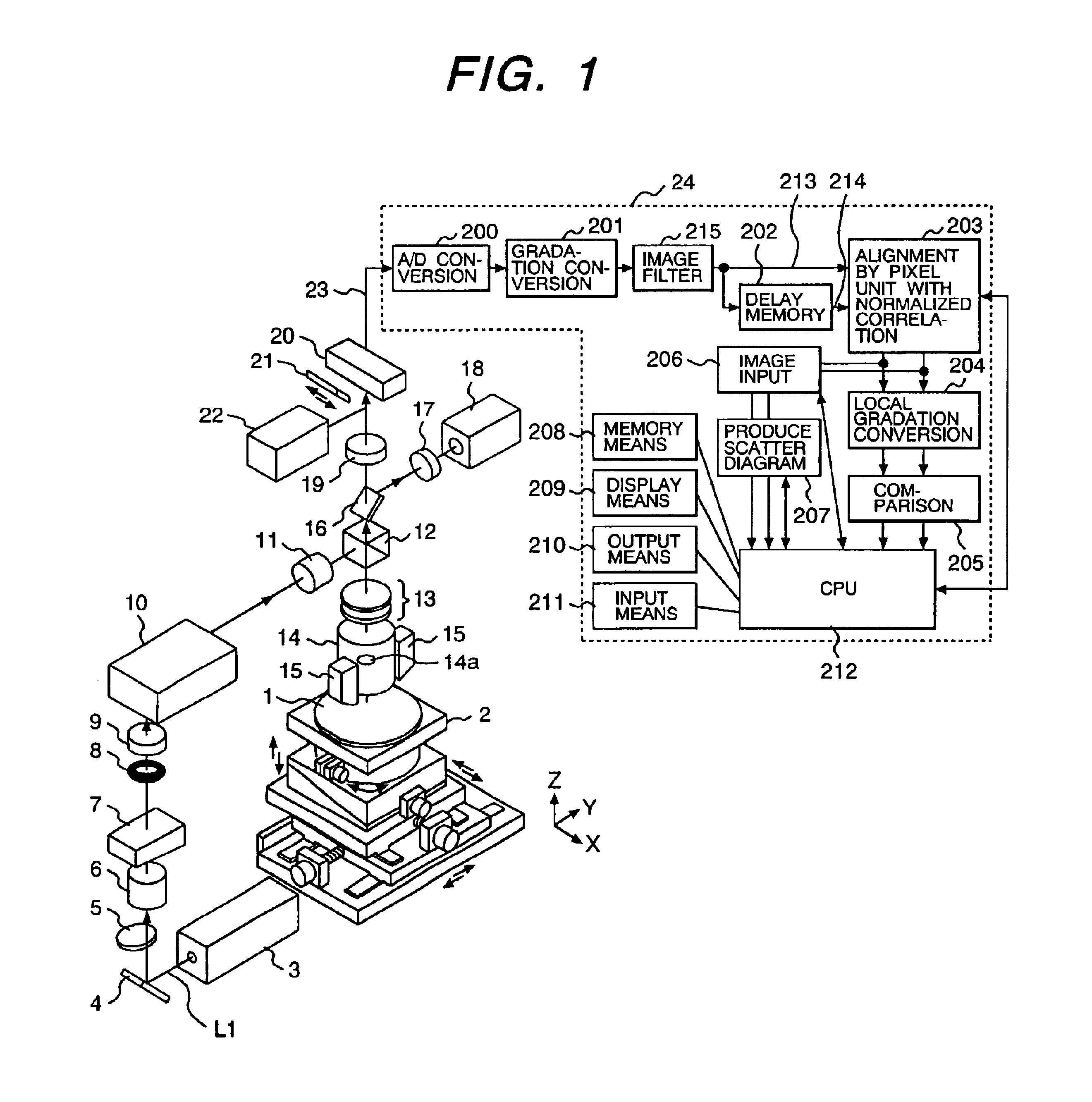
[0045]Hereinafter, embodiments, i.e., a method and an apparatus for inspecting defects on patterns to be tested, according to the present invention will be fully explained by referring to the attached drawings. FIG. 1 is a view for showing an embodiment of the apparatus according to the present invention. A stage 2 is built up with X, Y, Z and θ (rotation) stages, and this stage 2 is mounted a pattern to be tested or examined, such as, a semiconductor water (sample) 1, for an example. An illumination light source 3 is built up with, such as, a UV laser beam source irradiating the laser beam having wavelength of 266 nm or 355 nm therefrom, i.e., it is a light source for illumination of a sample 1. As such the UV laser beam source, it may be built up with a device of generating a third high-harmonic (355 nm) or a fourth high-harmonic (266 nm) of a basic wavelength, in which a laser beam from a solid YAG laser is converted in the wavelength thereof through a non-linear optical crystal,...


PUM

PropertyMeasurementUnit
diameteraaaaaaaaaa
diameteraaaaaaaaaa
sizeaaaaaaaaaa

Abstract

An apparatus for inspecting pattern defects on microscopic circuit patterns, with high resolution, comprises: an objective lens for detecting an image of a sample; a UV laser beam illumination arrangement for illuminating onto a pupil of the objective lens; am arrangement for lowering coherency of the UV laser illumination; a detector of integration type; and an arrangement for processing detected signal thereof.

Description

BACKGROUND OF THE INVENTION[0001]The present invention relates to inspection of patterns and / or foreign matters, for detecting or examining defects, such as short-circuit and / or open-circuit or the like, on the patterns as a target of inspection, and relates, in particular, to a method and an apparatus, for inspecting the defects and / or foreign matters of the patterns formed on, such as, a semiconductor wafer, a liquid crystal display, and a photo-mask, etc., for example. Hereinafter, it is assumed that the defects include the foreign matters, in the meaning thereof.[0002]Conventionally, in such kind of an inspection apparatus, as is described in Japanese Patent Laying-Open No. Hei 7-318326 (1995) <hereinafter, conventional art 1>, an image is detected on the patterns to be examined or inspected by means of an image pick-up element, such as a line sensor, etc., while moving the patterns to be inspected, so as to compare an image signal detected with one which is delayed by a p...

Claims


Application Information

Patent Timeline
Patent Type & Authority Patents(United States)
IPC IPC(8): G01N21/88G01N21/956G01N21/00G01N21/95
CPCG01N21/95607G01N21/95684G01N21/9501G01N2021/9513
Inventor YOSHIDA, MINORUMAEDA, SHUNJISHIMODA, ATSUSHISAKAI, KAORUOKABE, TAKAFUMI
Owner HITACHI LTD
Why Eureka
Try Eureka