Apparatus for and method of controlling AIVC through block selection information in semiconductor memory device

a technology of aivc and memory device, which is applied in the direction of information storage, static storage, digital storage, etc., can solve the problems of power loss and excess power consumption, and achieve the effect of preventing or reducing the possibility of bank voltage overshooting

Inactive Publication Date: 2005-08-09
SAMSUNG ELECTRONICS CO LTD
View PDF6 Cites 11 Cited by
  • Summary
  • Abstract
  • Description
  • Claims
  • Application Information

AI Technical Summary

Benefits of technology

[0016]Exemplary embodiments of the present invention provide a bank voltage control apparatus using block information, to prevent or reduce the possibility of a bank voltage from overshooting by supplying a voltage corresponding to a position of an array block of a bank.
[0017]In another exemplary embodiment, the present invention is directed to a bank voltage control apparatus using block information, to reduce power consumption by determining a driver size and a drive time of an over driver according to a block position through activated block information.

Problems solved by technology

The respective voltage generators which generate the additional voltages cause a power loss, in particular, the substrate bias voltage and the word line voltage.
Thus, a power overshoot is caused in the first array block 31 near to the 1st through 8th AIVC drivers 21˜28 and excess power consumption is caused due to a large capacity of the AIVC drivers.

Method used


Image

  • Apparatus for and method of controlling AIVC through block selection information in semiconductor memory device
  • Apparatus for and method of controlling AIVC through block selection information in semiconductor memory device
  • Apparatus for and method of controlling AIVC through block selection information in semiconductor memory device

Examples


Embodiment Construction

[0031]Hereinafter, exemplary embodiments of the present invention will be described in detail with reference to FIGS. 3 trough 5. In the inventive description, details of widely known functions of constructions will be omitted so as not to obscure the gist of the present invention.

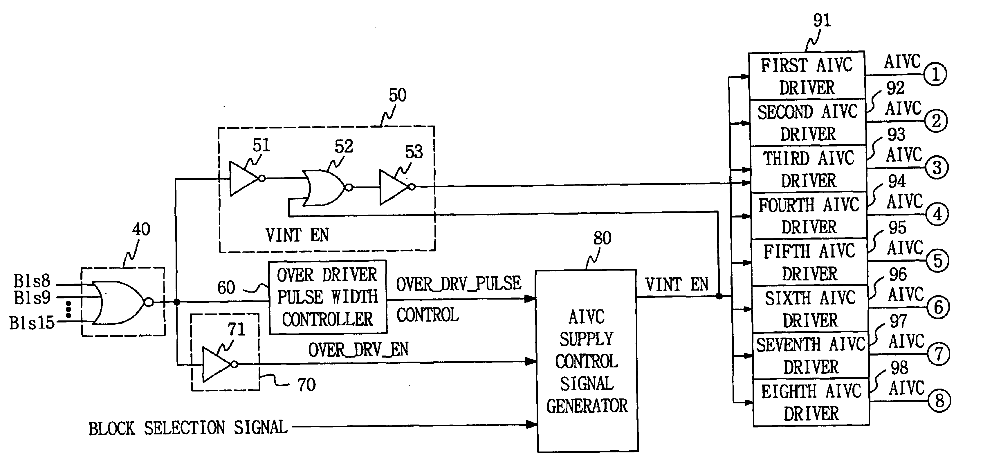
[0032]FIGS. 3A AND 3B illustrate a block diagram of a bank voltage control apparatus using block information in accordance with an exemplary embodiment of the present invention.

[0033]Referring first to FIGS. 3A AND 3B, the bank voltage (AIVC) control apparatus includes an array block signal detector 40, an oversize driver controller 50, an over driver pulse width controller 60, an over driver enable signal generator 70, an AIVC supply control signal generator 80, 1st through 8th AIVC drivers 91˜98, and a memory bank 100.

[0034]The array block signal detector 40 receives, inverts and logically sums block selection signals Bls8˜Bls15 for blocks Block8˜Block15 disposed distant from an AIVC driver, and then pro...


PUM


Abstract

A method of controlling a bank voltage (AIVC) through memory block selection information, said method comprising the steps of detecting an array block selection signal of an array block disposed distantly from an AIVC driver in response to an activated memory array block selection signal; and supplying a second bank voltage to a memory bank by driving a normal size driver and an oversize driver when detecting the array block selection signal for the distantly disposed array block.

Description

[0001]This U.S. nonprovisional patent application claims priority under 35 U.S.C. § 119 of Korean Patent Application 2002-69613 filed on Nov. 11, 2002, the entire contents of which is hereby incorporated by reference.FIELD OF THE INVENTION[0002]The present invention relates to a semiconductor memory device, and more particularly, to AIVC control apparatus and method to selectively supply a bank voltage.DESCRIPTION OF THE RELATED ART[0003]A semiconductor memory device generally includes numerous memory cells. According to U.S. Pat. No. 5,109,265 based on a conventional technology of the semiconductor memory device having such numerous cells, the plurality of memory cells are divided into four memory banks. To provide a supply voltage, different additional voltages are generated in the semiconductor memory device which are then supplied to memory cells.[0004]For example, a substrate bias voltage is supplied to a substrate, a word line voltage is supplied to a word line of a memory ban...

Claims


Application Information

Patent Timeline
Patent Type & Authority Patents(United States)
IPC IPC(8): G11C5/14G11C8/00G11C8/12G11C5/06G11C7/00
CPCG11C5/063G11C5/14G11C8/12G11C7/00
Inventor LEE, HO-CHEOLRYOO, JUNG-SOO
Owner SAMSUNG ELECTRONICS CO LTD
Why Eureka
Try Eureka