Semiconductor component having test contacts

a technology of semiconductor components and test contacts, which is applied in the direction of individual semiconductor device testing, semiconductor/solid-state device testing/measurement, instruments, etc., can solve the problems of contamination of equipment used to conduct test procedures, contamination of interconnect contacts, and contamination of solder attracted contaminants

Inactive Publication Date: 2005-08-23
MICRON TECH INC
View PDF49 Cites 51 Cited by
  • Summary
  • Abstract
  • Description
  • Claims
  • Application Information

AI Technical Summary

Benefits of technology

[0024]An alternate embodiment test system includes a carrier configured to temporarily package one or more singulated components in electrical communication with the interconnect.

Problems solved by technology

However, as this ideal situation does not always exist, redistribution circuits are widely used in semiconductor manufacture.
Regardless of the type of interconnect, problems can arise in making the temporary electrical connections with the bumped contacts 14.
These flakes can contaminate the equipment used to conduct the test procedures.
In addition, solder, and contaminants attracted to the solder, can build up on the interconnect contacts.
This build up can increase electrical resistivity through the contacts, and adversely affect the test procedures.
Another problem during testing of bumped components, particularly with bumped contacts 14 formed of solder, is that the bumped contacts 14 deform easily during handling and testing, especially at elevated temperatures.
For performing test procedures, it may be difficult to make low resistance electrical connections with deformed bumped contacts 14.
Also for subsequent bonding procedures, the deformed bumped contacts 14 can make alignment and bonding of the component to a mating substrate more difficult.
In addition, deformed bumped contacts 14 are a cosmetic problem that can adversely affect a users perception of a semiconductor component.

Method used


Image

  • Semiconductor component having test contacts
  • Semiconductor component having test contacts
  • Semiconductor component having test contacts

Examples


Embodiment Construction

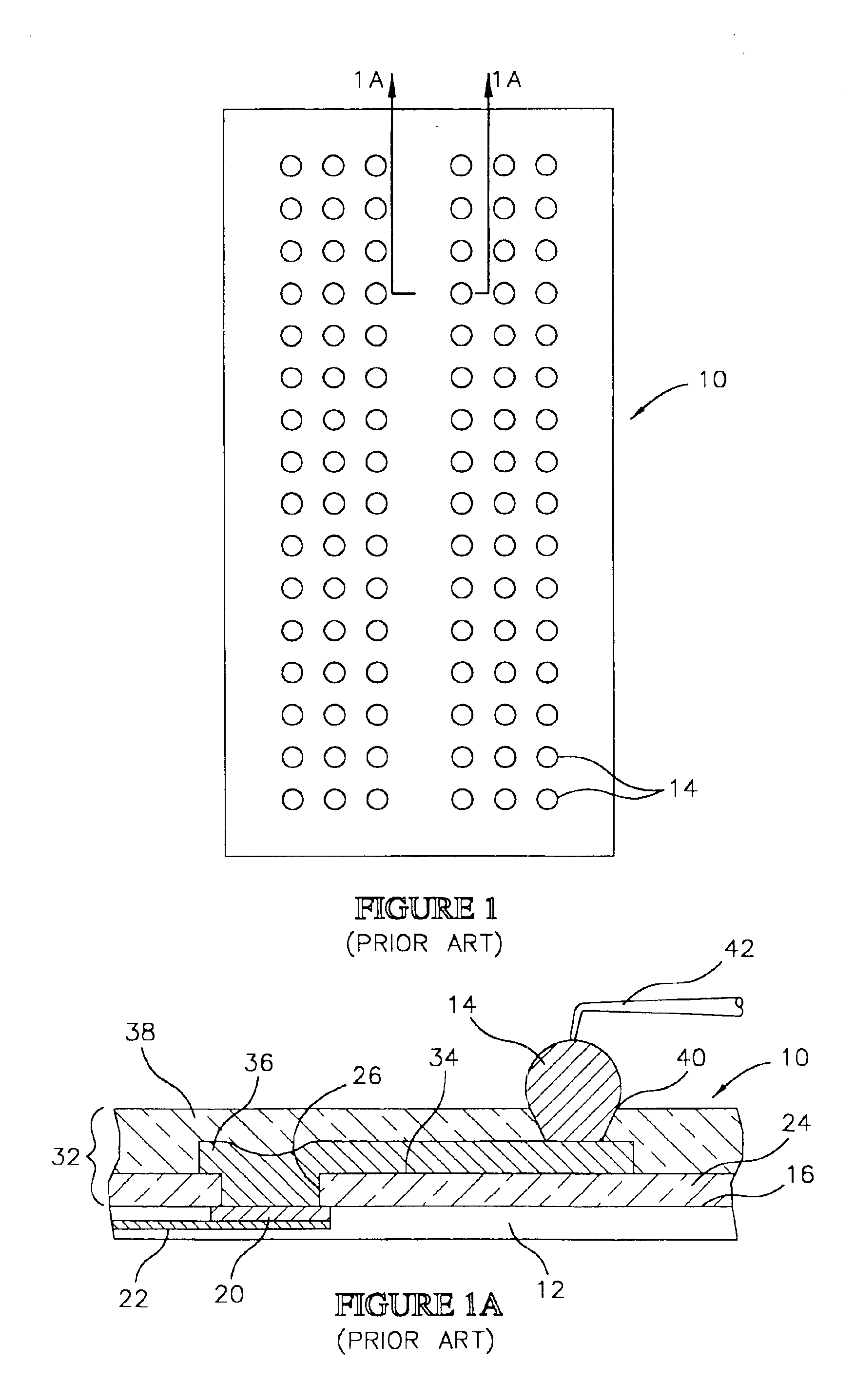
[0046]As used herein, the term “semiconductor component” refers to an electronic component that includes a semiconductor die. Exemplary semiconductor components include bare semiconductor dice, chip scale packages, ceramic or plastic semiconductor packages, BGA devices, semiconductor wafers, and panels and leadframes containing multiple dice or chip scale packages.

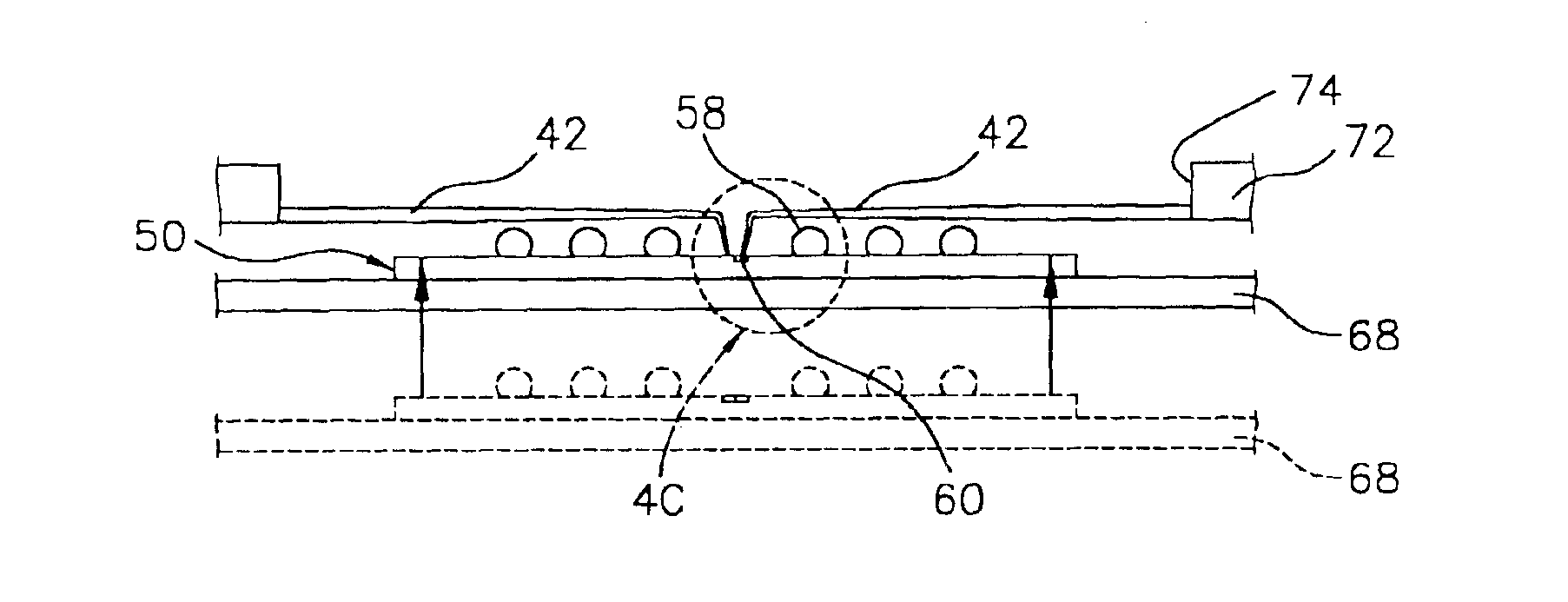
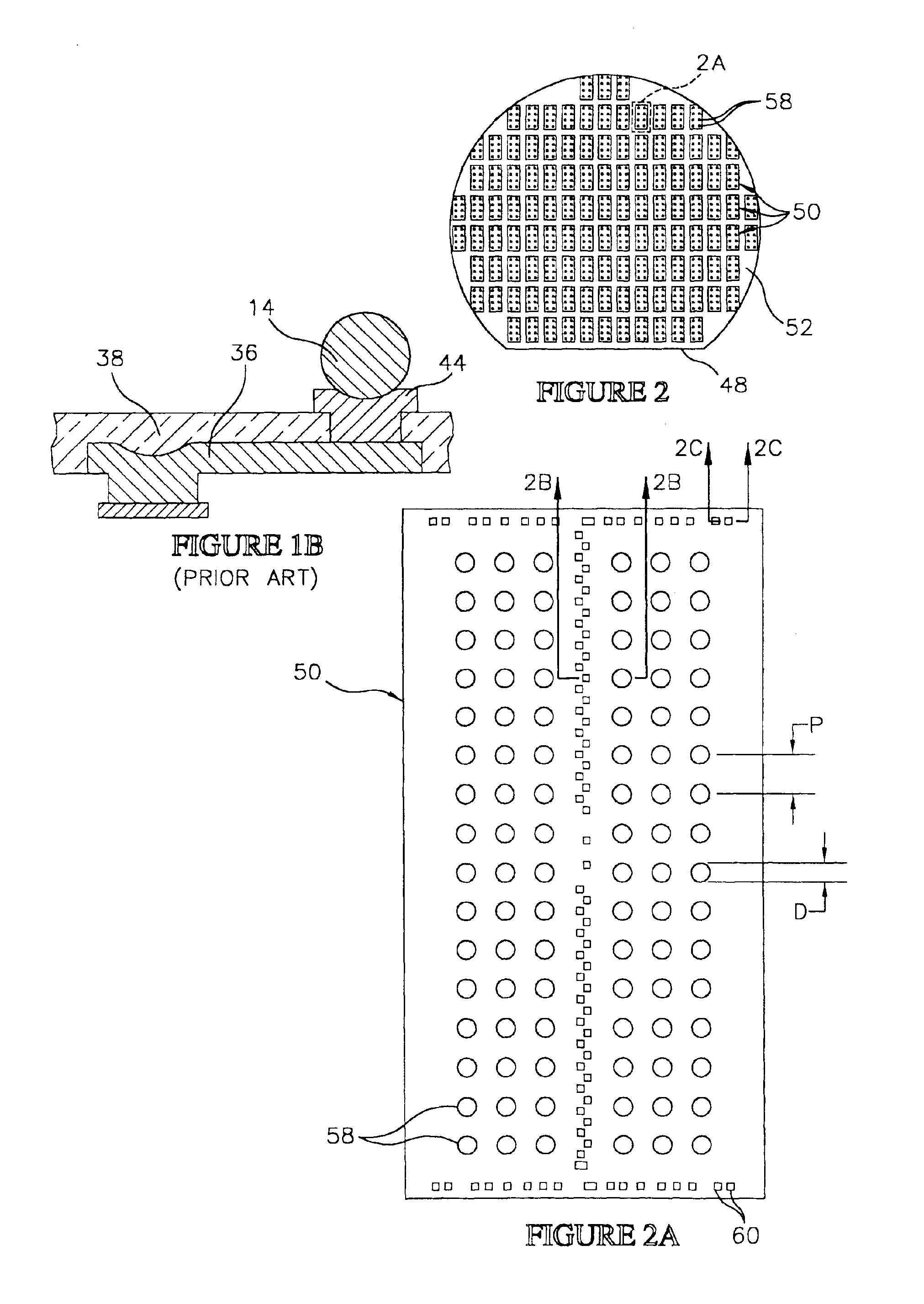
[0047]Referring to FIGS. 2-2C, a bumped semiconductor component 50 constructed in accordance with the invention is illustrated. As shown in FIG. 2, the semiconductor component 50 can be contained on a wafer 52 which comprises a plurality of components 50. Although the wafer 52 is illustrated as being generally circular in shape with a major flat, the semiconductor component 50 can be contained on a wafer, or portion thereof, having a different shape than the wafer 52. The component 50 can also be contained on a panel, or on a leadframe.

[0048]Alternately, the semiconductor component 50 can be a singulated component which ha...


PUM


Abstract

A bumped semiconductor component includes bumped contacts, a semiconductor die having die contacts, and a redistribution circuit having conductors for establishing electrical communication between the die contacts and the bumped contacts. The redistribution circuit also includes test contacts in electrical communication with the die contacts and with the bumped contacts. The test contacts allow the die to be tested without electrical engagement of the bumped contacts. The bumped semiconductor component can be contained on a wafer, or can be a singulated component such as a flip chip package. A test system includes the bumped semiconductor component, and an interconnect having contacts configured to electrically engage the test contacts without interference from the bumped contacts. If the test contacts are aligned with the die contacts, the same interconnect can be used to test the bare die as well as the bumped component. A test method includes the steps of: providing the bumped component with test contacts; providing the interconnect with interconnect contacts configured to engage the test contacts without interference from the bumped contacts; and then testing the component by applying test signals through the interconnect contacts to the test contacts.

Description

CROSS REFERENCE TO RELATED APPLICATIONS[0001]This application is a continuation of Ser. No. 09 / 835,200, filed Apr. 13, 2001, U.S. Pat. No. 6,620,633, which is a division of Ser. No. 09 / 473,232, filed Dec. 24, 1999, U.S. Pat. No. 6,380,555 B1.FIELD OF THE INVENTION[0002]This invention relates generally to semiconductor manufacture and testing. More particularly, this invention relates to a bumped semiconductor component having test pads, and to a method and system for testing bumped semiconductor components.BACKGROUND OF THE INVENTION[0003]Semiconductor components, such as bare semiconductor dice, semiconductor packages, chip scale packages, BGA devices, and semiconductor wafers can include terminal contacts in the form of bumps. This type of component is sometimes referred to as a “bumped” component (e.g., bumped die, bumped package, bumped wafer).[0004]FIGS. 1 and 1A illustrate a bumped semiconductor component which comprises a “flip chip” semiconductor package 10. The package 10 i...

Claims


Application Information

Patent Timeline
Patent Type & Authority Patents(United States)
IPC IPC(8): H01L23/52H01L23/58H01L23/528
CPCH01L22/32H01L23/528H01L2224/13022H01L2224/05001H01L2224/05027H01L2224/05569H01L2224/05024H01L2224/05022H01L2224/05548H01L2224/05567H01L2224/05023H01L2224/05572H01L2224/0392H01L2224/0615H01L24/05H01L2224/023H01L2924/0001
Inventor HEMBREE, DAVID R.DE VARONA, JORGE L.
Owner MICRON TECH INC
Why Eureka
Try Eureka