Interconnection structure with etch stop

a technology of interconnection structure and etch stop, which is applied in the direction of waveguide devices, basic electric elements, and metal adhesion improvement of insulation substrates, can solve the problems of limited packaging with respect to optical or acoustic sensors that cannot operate efficiently, adversely affect devices, etc., and achieve high pin count interconnections

Inactive Publication Date: 2005-08-23
GENERAL ELECTRIC CO
View PDF5 Cites 15 Cited by
  • Summary
  • Abstract
  • Description
  • Claims
  • Application Information

AI Technical Summary

Problems solved by technology

Thus such packaging has been limited with respect to optical or acoustic sensors that cannot operate efficiently when covered by material which attenuates or distorts energy transmission.
As described in Kornrumpf et al., U.S. Pat. No. 5,355,102, issued 11 Oct. 1994, ablating dielectric material over the center of a device may adversely affect the device.

Method used


Image

  • Interconnection structure with etch stop
  • Interconnection structure with etch stop
  • Interconnection structure with etch stop

Examples


Embodiment Construction

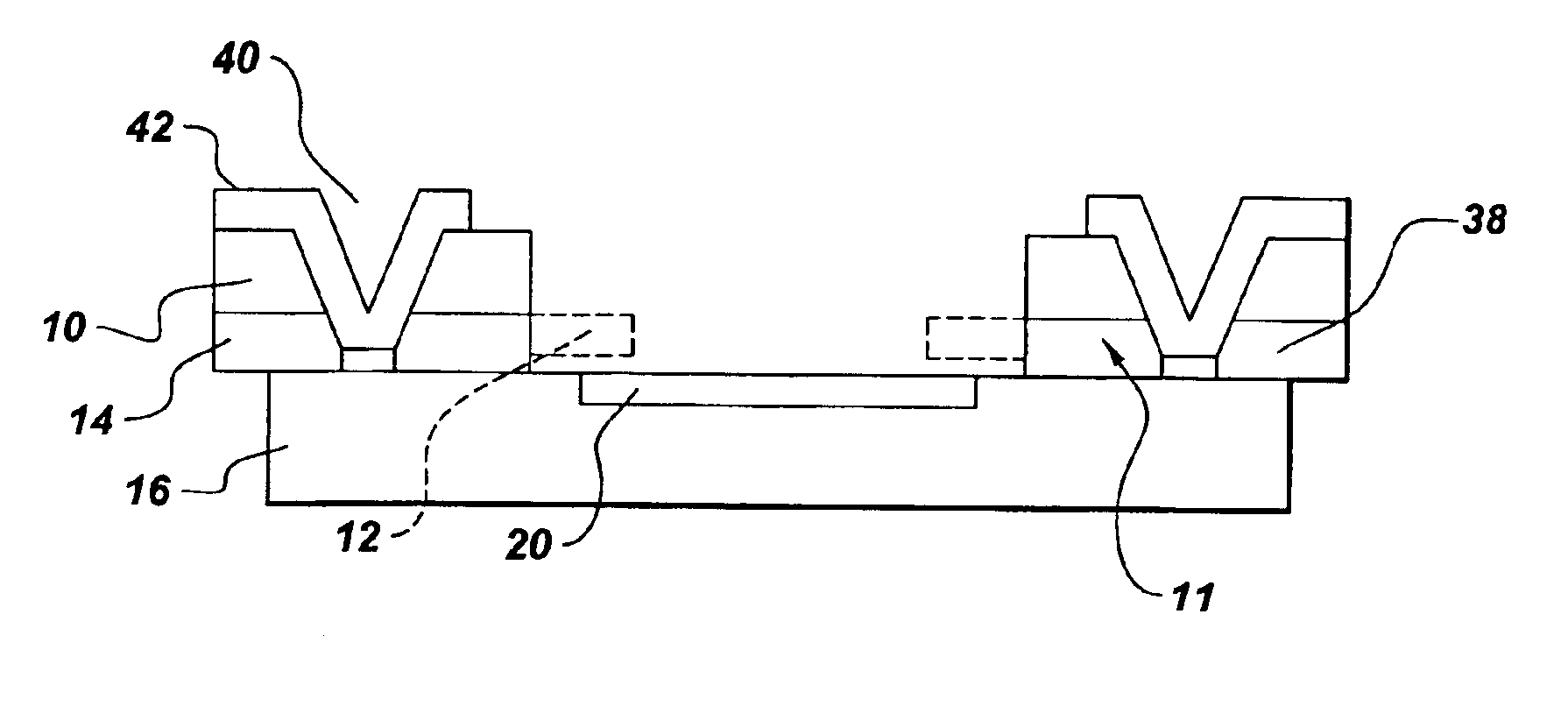
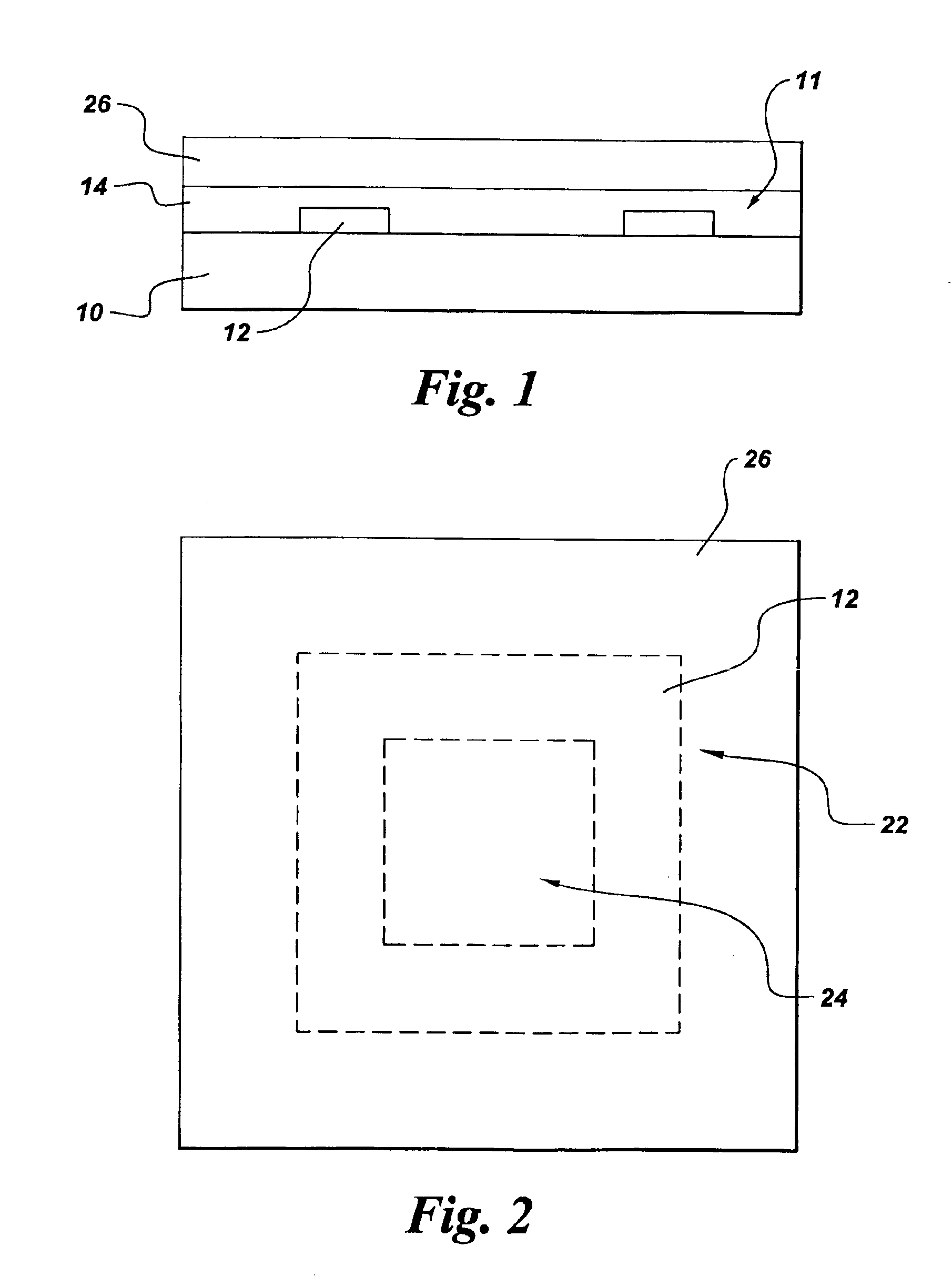
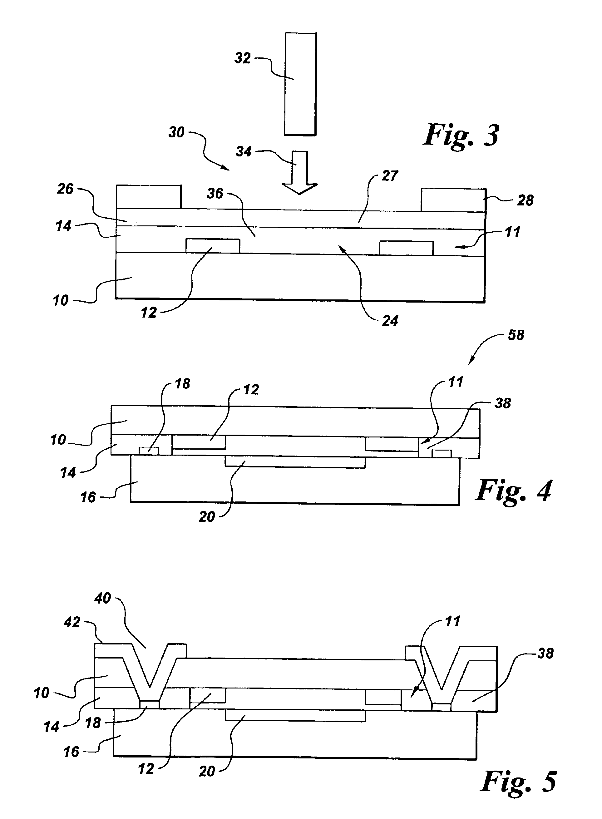
[0020]FIGS. 1 and 2 are sectional side and top views of a dielectric layer 10, (FIG. 1) a metallization pattern 11, (FIG. 1) an adhesive 14, (FIG. 1) and a cover sheet 26 for use in accordance with one embodiment of the present invention; FIGS. 3-6 are sectional side views of further processing stages in accordance with the embodiment of FIG. 1; and FIG. 7 is a partial top view illustrating one embodiment for use in obtaining the embodiment of FIG. 6.

[0021]Briefly, in one example embodiment, an interconnection method comprises: applying a first metallization pattern 11 on a dielectric layer 10, the first metallization pattern including at least one etch stop 12 (FIG. 1,2) having a perimeter 22 (FIG. 1) defining at least one etch stop opening 24 (FIGS. 1); using an adhesive 14 to attach a protective cover sheet 26 over the first metallization pattern and the dielectric layer (FIG. 1); aligning at least one mask opening 30 with the at least one etch stop opening (FIG. 3); removing a f...


PUM

PropertyMeasurementUnit
thicknessaaaaaaaaaa
thicknessaaaaaaaaaa
thicknessaaaaaaaaaa

Abstract

An interconnection structure includes: a dielectric layer; a first metallization pattern on the dielectric layer, the first metallization pattern including at least one etch stop having a perimeter defining at least one etch stop opening; a cured adhesive on a portion of the dielectric layer, the adhesive not present in an area aligned with the at least one etch stop; and at least one electrical device being attached to the dielectric layer by the adhesive such that an active area of the at least one electrical device is aligned with the etch stop perimeter. The active area of the at least one electrical device may further be aligned with at least one predetermined area defined by an optional additional portion of cured adhesive, the additional portion of the cured adhesive being adhesively attached to the dielectric layer and not adhesively attached to the at least one electrical device.

Description

[0001]This application is a divisional of application Ser. No. 09 / 681,066 filed Dec. 18, 2000 now U.S. Pat. No. 6,671,948.BACKGROUND OF INVENTION[0002]The invention relates generally to electrical device packaging and more to packaging of electrical devices requiring energy transmission to and / or from device active areas.[0003]As the need for smaller, lighter, portable and / or mobile equipment increases in applications such as medical imaging, consumer electronics, and communication devices, the need for high density device and system level packaging likewise increases. High density packages would be most beneficial if adapted for interconnecting hundreds of input and output pads and providing an unobstructed path for transmission and / or absorption of energy directed to and / or from the active area of a packaged device.[0004]For example, ultrasound imaging equipment uses active areas of electrical devices to transmit and receive hundreds of acoustic signals which can be used to create...

Claims


Application Information

Patent Timeline
Patent Type & Authority Patents(United States)
IPC IPC(8): H01L23/34H01L21/02H01L23/538H01L23/50H01L21/60H01L23/52H01L23/12H01L21/3205H01L23/48H01P1/04H05K3/06H05K3/38H01HH01L21/48
CPCH01L24/82H01L27/14636H01L24/19H01L27/14618Y10T29/49156H01L2224/18H01L2224/92144H01L2924/01004H01L2924/01013H01L2924/01027H01L2924/01029H01L2924/01033H01L2924/014Y10T29/49155Y10T29/49165H01L2924/12042H01L2224/04105H01L2924/00
Inventor BURDICK, JR., WILLIAM EDWARDROSE, JAMES WILSONDUROCHER, KEVIN MATTHEWFILLION, RAYMOND ALBERT
Owner GENERAL ELECTRIC CO
Why Eureka
Try Eureka