Integrated circuits with temperature-change and threshold-voltage drift compensation
- Summary
- Abstract
- Description
- Claims
- Application Information
AI Technical Summary
Benefits of technology
Problems solved by technology
Method used
Image
Examples
Embodiment Construction
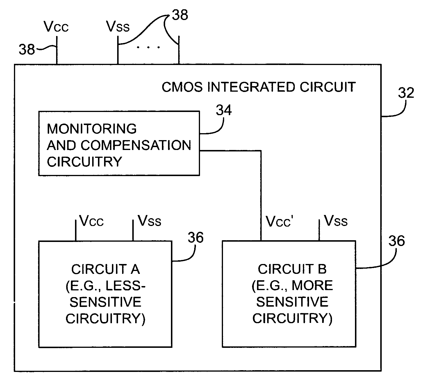
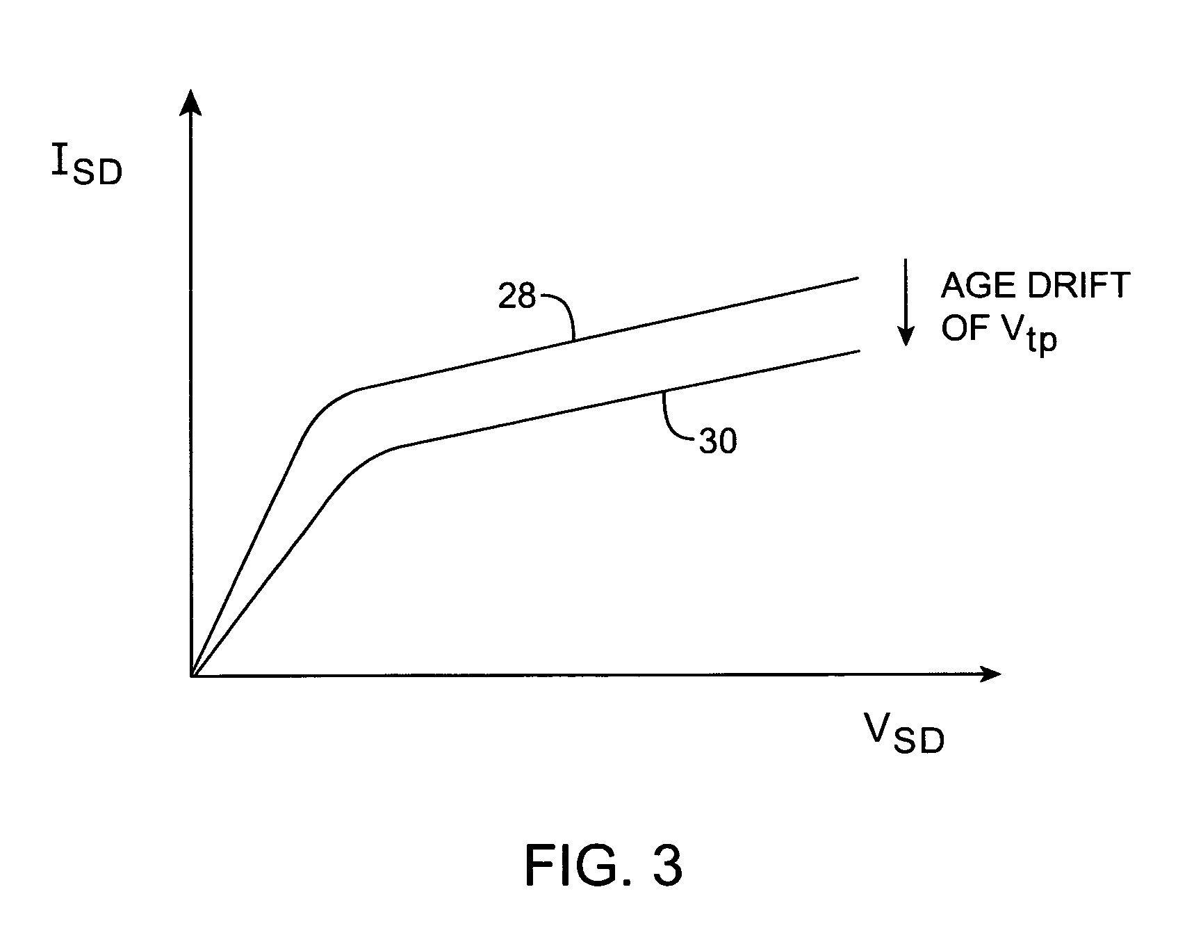
[0029]The present invention relates to complementary metal-oxide-semiconductor (CMOS) integrated circuits having n-channel metal-oxide-semiconductor (NMOS) transistors and p-channel metal-oxide-semiconductor (PMOS) transistors. The invention also relates to circuitry and methods for ensuring proper operation of CMOS integrated circuits that are exposed to changes in temperature and changes in transistor threshold voltages due to aging.
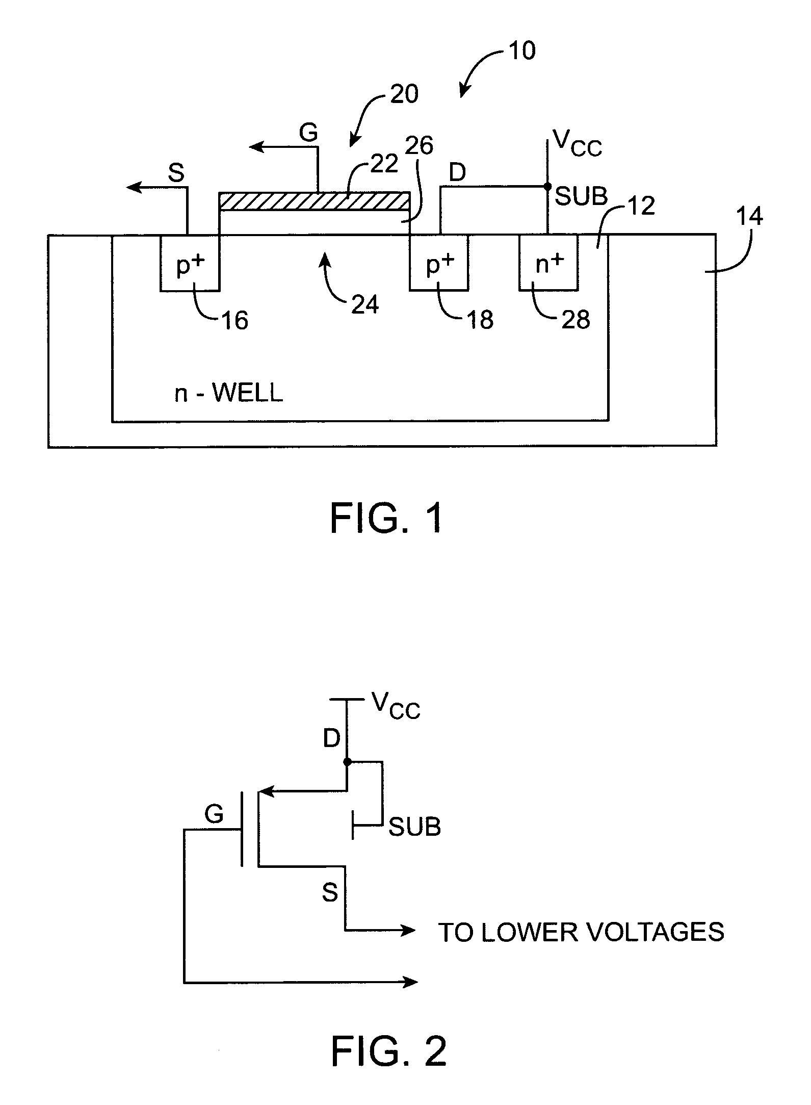
[0030]A cross-section of a typical PMOS transistor 10 on a CMOS integrated circuit is shown in FIG. 1. Transistor 10 may be formed in an n-type well 12 on a silicon substrate 14. Heavily-doped p+ regions are used to form a source 16 (S) and drain 18 (D). The transistor is controlled by applying signals to gate 20 (G). Gate 20 has a gate conductor 22, which is separated from an underlying channel region 24 in well 12 by a gate oxide 26. A heavily-doped n+ region 28 is used to form a “substrate” or bulk contact (SUB).
[0031]Transistors such as transistor ...
PUM
 Abstract
Description
Claims
Application Information
 - R&D
- Intellectual Property
- Life Sciences
- Materials
- Tech Scout
- Unparalleled Data Quality
- Higher Quality Content
- 60% Fewer Hallucinations
Browse by: Latest US Patents, China's latest patents, Technical Efficacy Thesaurus, Application Domain, Technology Topic, Popular Technical Reports.
© 2025 PatSnap. All rights reserved.Legal|Privacy policy|Modern Slavery Act Transparency Statement|Sitemap|About US| Contact US: help@patsnap.com


