Pixel driving circuit of an organic light emitting diode display panel

a technology of light-emitting diodes and driving circuits, which is applied in the direction of instruments, static indicating devices, etc., can solve the problems of low manufacturing cost and technical level of passive matrix type oleds (pmoleds), inability to expand the resolution of oleds, and complex manufacturing processes

Inactive Publication Date: 2005-08-30
WINTEK CORP
View PDF6 Cites 221 Cited by
  • Summary
  • Abstract
  • Description
  • Claims
  • Application Information

AI Technical Summary

Benefits of technology

[0013]It is a further object of the present invention to provide a voltage driving type active matrix OLED display panels having the threshold voltage of the TFT which can be compensated, and to improve the non-uniform image defect caused by uneven character of the threshold voltage of the TFTs.

Problems solved by technology

Although the manufacturing cost and the technical level of the passive matrix type OLED (PMOLED) are lower, the PMOLED is restricted by the driving method, and then the resolution of the OLED cannot be enlarged.
The differences between the LTPS TFT and the a-Si TFT are the electric characteristics of the TFT devices and the complexity of the manufacturing process.
The mobility of the carrier of the LTPS TFT is higher than that of the a-Si TFT and the higher mobility of the carrier means that the TFT can provide much more electric current under the same voltage bias, but the manufacturing process of the LTPS TFT is more complex.
For above reason, the result leads the OLED display panel to display an image with erroneous gray scale and to have bad image uniformity.
As described above, according to the U.S. Pat. No. 6,362,798, the requirement of the manufacturing process is higher, so as to be disadvantageous for the production yield of display panels.
According to the thesis, the requirement of the manufacturing process is also higher, so as to be disadvantageous for the production yield of display panels.

Method used


Image

  • Pixel driving circuit of an organic light emitting diode display panel
  • Pixel driving circuit of an organic light emitting diode display panel
  • Pixel driving circuit of an organic light emitting diode display panel

Examples


first embodiment

[0022]The

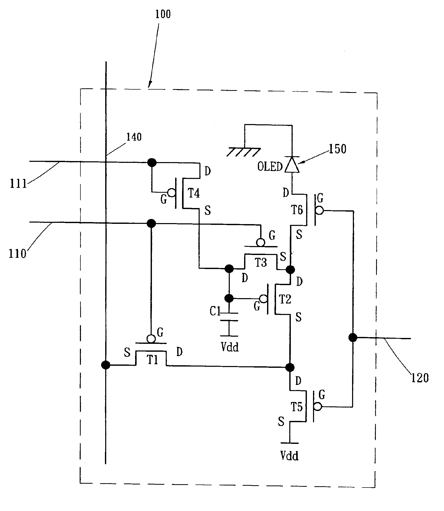
[0023]Referring to FIG. 1, it is the schematic view of a pixel driving circuit according to the present invention. Each scan line 110 and each data line 140, which are disposed on a display panel according to the present invention, crosswise constitute a pixel 100. The pixel driving circuit disposed on the pixel 100 includes:

[0024]a scan TFT T1, of which a gate (G) is connected to the scan line 110 and of which a source (S) is connected to the data line 140;

[0025]a Vdd-connected TFT T5, of which a source (S) is connected to a power supply (Vdd), of which a drain (D) is connected to the drain (D) of the scan TFT T1, and of which a gate (G) is connected to a light-emitting line 120 disposed on the pixel 100;

[0026]a driving TFT T2, of which a source (S) is connected to the drain (D) of the Vdd-connected TFT T5 and of which a drain (D) is connected to the source (S) of the OLED-connected TFT T6;

[0027]a diode-connected TFT T3, of which a source (S) is connected to the drain (D) ...

second embodiment

[0038]The

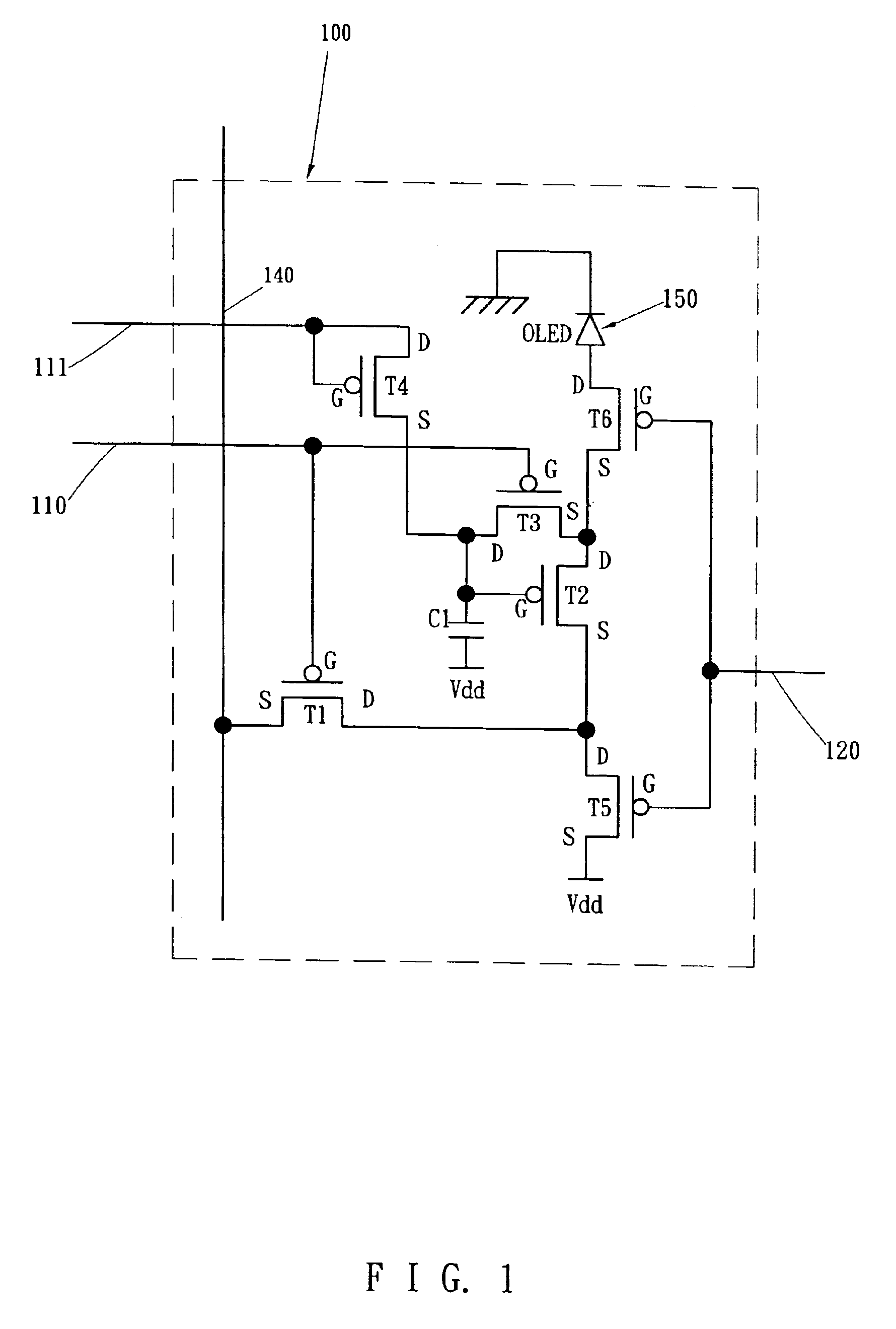
[0039]Referring to FIG. 2, it is the schematic view of another pixel driving circuit according to the present invention. Each scan line 110 and each data line 140, which are disposed on a display panel according to the present invention, crosswise constitute a pixel 100. The pixel driving circuit disposed on the pixel 100 includes:

[0040]a scan TFT T1, of which a gate (G) is connected to the scan line 110 and of which a source (S) is connected to the data line 140;

[0041]an OLED-connected TFT T6, of which a source (S) is connected to the drain (D) of the scan TFT T1 and of which a gate (G) is connected to the light-emitting line 120 of the pixel 100;

[0042]an OLED 150, of which one end is an anode and connected to the drain (D) of the OLED-connected TFT T6, and of which the other end is cathode and connected to ground;

[0043]a driving TFT T2, of which a drain (D) is connected to the drain (D) of the Vdd-connected TFT T5 and of which a source (S) is connected to the source (S) o...

third embodiment

[0055]The

[0056]Referring to FIG. 4, it is the schematic view of a further pixel driving circuit according to the present invention. Each scan line 110 and each data line 140, which are disposed on a display panel according to the present invention, crosswise constitute a pixel 100. The pixel driving circuit disposed on the pixel 100 includes:

[0057]a scan TFT T1, of which a gate (G) is connected to the scan line 110 and of which a source (S) is connected to the data line 140;

[0058]a driving TFT T2, of which a source (S) is connected to the drain (D) of the scan TFT T1 and is further connected to a power supply line 130;

[0059]a diode-connected TFT T3, of which a source (S) is connected to the drain (D) of the driving TFT T2 and of which a gate (G) is connected to the scan line 110, and used for making the driving TFT T2 formed a diode-connected type;

[0060]a storage capacitor C1, having one end is connected to the gate (G) of the driving TFT T2 and the drain (D) of the diode-connected ...


PUM


Abstract

A pixel driving circuit of an organic light emitting diode display panel includes a scan TFT, a Vdd-connected TFT, a driving TFT, a diode-connected TFT, a storage capacitor, a reset TFT, an OLED-connected TFT, and an organic light emitting diode. A reset TFT is connected to the diode-connected TFT and a previous scan line. An OLED-connected TFT is connected to the driving TFT and the light-emitting line. An organic light emitting diode is connected to the OLED-connected TFT and the ground. The amount of output current to the OLED does not depend on the threshold voltage of the driving TFT and only depends on the amount of the data signal voltage to be written. Thus, the variance in the threshold voltage of the driving TFT caused by the factor of the manufacturing process can be compensated to improve the non-uniform image defect.

Description

FIELD OF THE INVENTION[0001]The present invention relates to a pixel driving circuit of an organic light emitting diode display panel and, more particularly, to a pixel driving circuit can improve the image uniformity of the active matrix type organic light emitting diode display panel with low temperature poly-silicon thin firm transistors.BACKGROUND OF THE INVENTION[0002]According to the driving types for organic light emitting diode (mentioned as OLED hereafter) displays, the OLED displays are divided into passive matrix type OLED (mentioned as PMOLED hereafter) and active matrix type OLED (mentioned as AMOLED hereafter). The so-called active matrix type OLED (AMOLED) utilizes thin film transistors (mentioned as TFT hereafter) and capacitors to store signals and thereby controls the brightness and the gray scale of the OLED.[0003]Although the manufacturing cost and the technical level of the passive matrix type OLED (PMOLED) are lower, the PMOLED is restricted by the driving meth...

Claims


Application Information

Patent Timeline
Patent Type & Authority Patents(United States)
IPC IPC(8): G09G3/32
CPCG09G3/3233G09G2300/0465G09G2300/0819G09G2300/0842G09G2300/0861G09G2320/043
Inventor LO, SHIN-TAI
Owner WINTEK CORP
Why Eureka
Try Eureka