Apparatus and method for collecting impurities on a semiconductor wafer

a technology of impurities and apparatus, which is applied in the direction of testing semiconductor materials, cleaning using liquids, instruments, etc., can solve the problems of deterioration in the performance of semiconductor devices, lower yields in semiconductor device manufacturing, and the inability of the apparatus to collect impurities from the edge portion of the semiconductor wafer

Active Publication Date: 2005-09-06
SAMSUNG ELECTRONICS CO LTD
View PDF8 Cites 7 Cited by
  • Summary
  • Abstract
  • Description
  • Claims
  • Application Information

AI Technical Summary

Problems solved by technology

The impurities cause deterioration in the performance of the semiconductor devices, as well as lower yields in the manufacturing of the semiconducto

Method used


Image

  • Apparatus and method for collecting impurities on a semiconductor wafer
  • Apparatus and method for collecting impurities on a semiconductor wafer
  • Apparatus and method for collecting impurities on a semiconductor wafer

Examples


Embodiment Construction

[0044]Korean Patent Application No. 2003-11109, filed on Feb. 21, 2003, and entitled: “Apparatus and Method For Collecting Impurities on a Semiconductor Wafer,” is incorporated by reference herein in its entirety.

[0045]The present invention now will be described more fully hereinafter with reference to the accompanying drawings, in which preferred embodiments of the invention are shown. This invention may, however, be embodied in many different forms and should not be construed as limited to the embodiments set forth herein; rather, these embodiments are provided so that this disclosure will be thorough and complete, and will fully convey the scope of the invention to those skilled in the art.

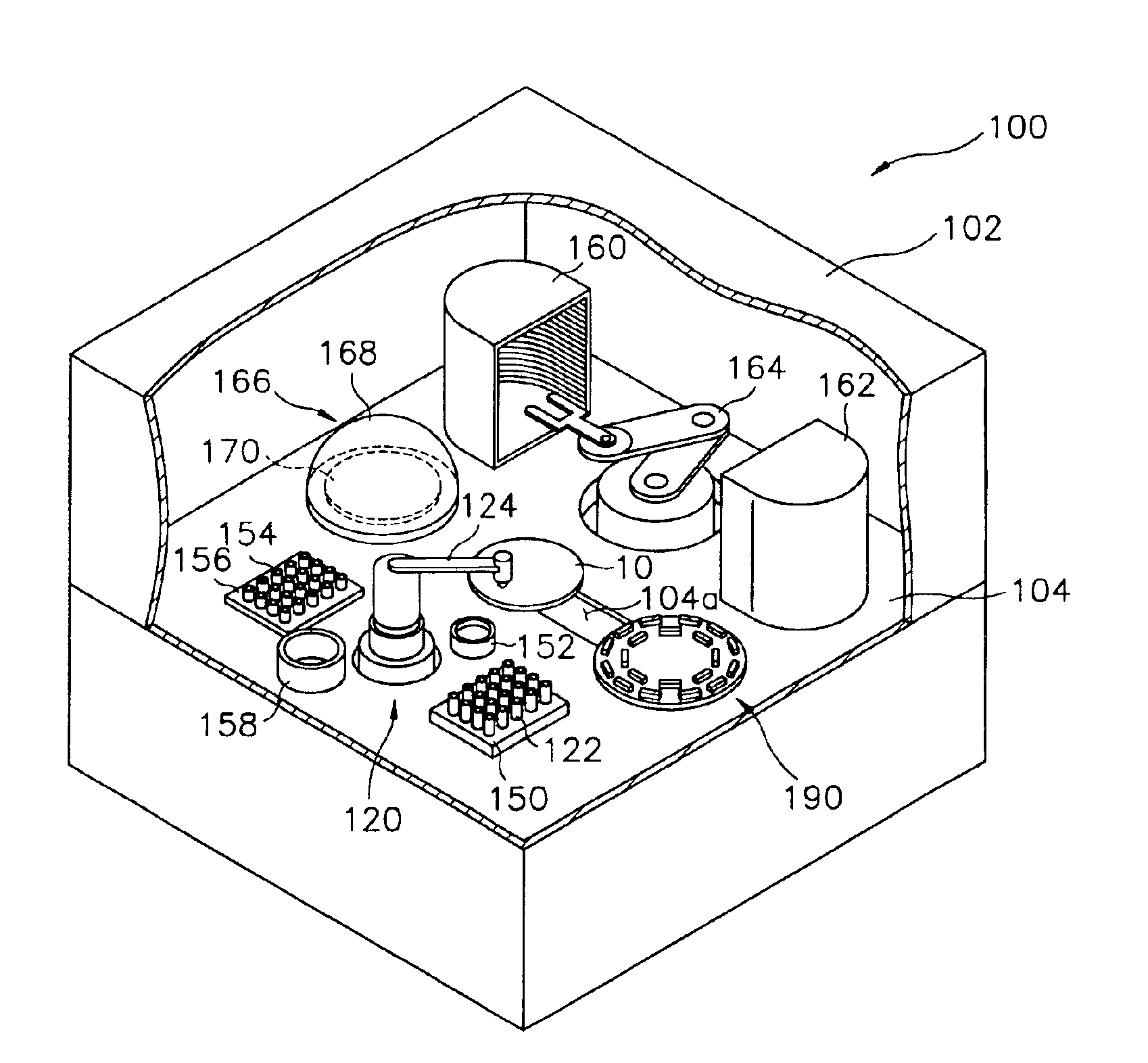
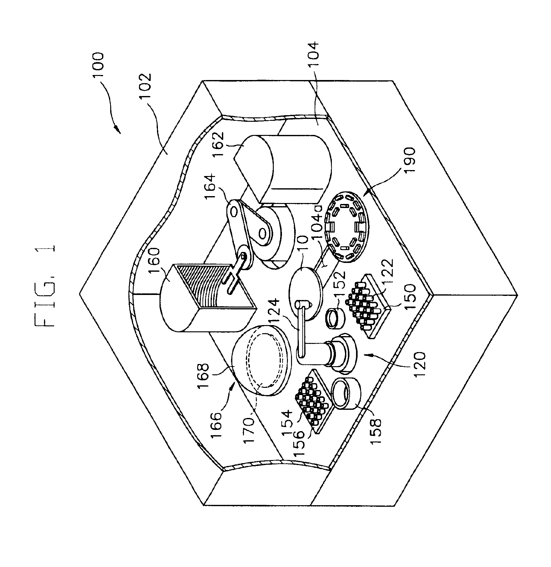
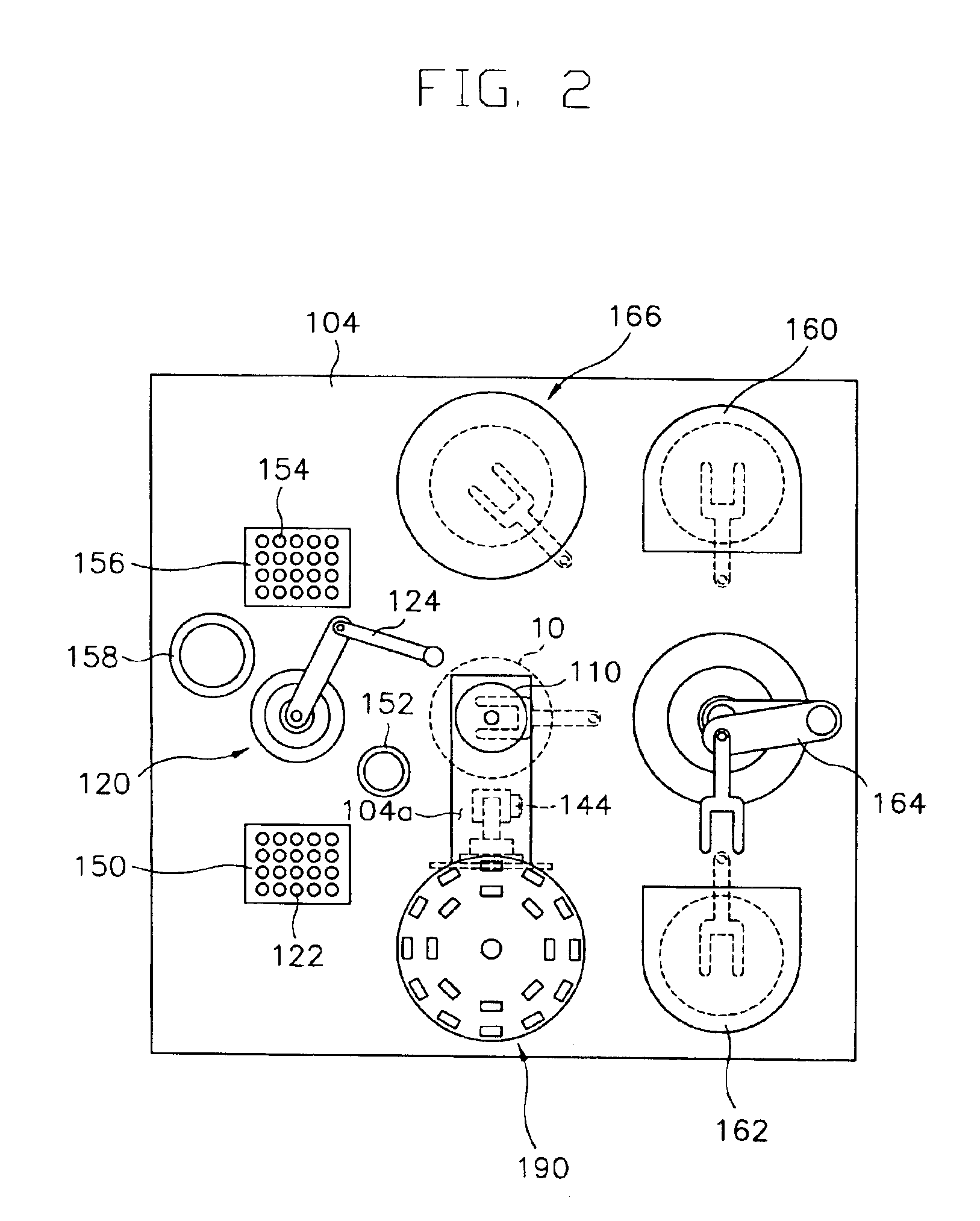
[0046]FIG. 1 illustrates a perspective view of an apparatus for collecting impurities according to one embodiment of the present invention. FIG. 2 illustrates a plan view of the apparatus for collecting impurities shown in FIG. 1.

[0047]Referring to FIGS. 1 and 2, an apparatus 100 for collecting...


PUM

PropertyMeasurementUnit
Pressureaaaaaaaaaa

Abstract

An apparatus for collecting impurities on a semiconductor wafer includes an airtight process chamber, a rotary chuck disposed in the process chamber for rotating and horizontally supporting the semiconductor wafer, a first scanning unit for forming a droplet of a first scanning solution and for scanning an upper surface of the semiconductor wafer rotated by the rotary chuck with the droplet to collect first impurities, a driving unit for tilting the rotary chuck and the semiconductor wafer supported on the rotary chuck, and a second scanning unit for receiving a second scanning solution for collecting second impurities from an edge portion of the semiconductor wafer, the second scanning solution being in contact with the edge portion of the semiconductor wafer tilted by the driving unit and rotated by the rotary chuck so that the second scanning solution scans the edge portion of the semiconductor wafer.

Description

BACKGROUND OF THE INVENTION[0001]1. Field of the Invention[0002]The present invention relates to an apparatus and a method for collecting impurities on a semiconductor wafer. More particularly, the present invention relates to an apparatus and a method for collecting metallic impurities remaining on a semiconductor wafer using a scanning solution.[0003]2. Description of the Related Art[0004]Generally, semiconductor devices are manufactured through a three-step process. First, a fabrication process is performed for forming electronic circuits on a semiconductor wafer. Second, an electrical die sorting (EDS) process is performed for inspecting electrical characteristics of the semiconductor devices on the semiconductor wafer. Third, a packaging process is performed for packaging the semiconductor devices in epoxy resins and individuating the semiconductor devices.[0005]The fabrication process may include a deposition process for depositing a layer on the semiconductor wafer, a chemica...

Claims


Application Information

Patent Timeline
IPC IPC(8): G01N1/02H01L21/00G01N33/00G01N1/40G01N35/00H01L21/02
CPCG01N1/02H01L21/6715G01N1/4044G01N35/0099G01N2001/028G01N2033/0095G01N2035/00059Y10S134/902H01L21/02
Inventor KO, YONG-KYUNSON, BYUNG-WOOJEONG, JONG-CHEOL
Owner SAMSUNG ELECTRONICS CO LTD
Why Eureka
Try Eureka