Semiconductor light-emitting element and method of manufacturing the same

a technology of semiconductors and light-emitting elements, applied in semiconductor devices, lasers, semiconductor lasers, etc., can solve the problems of increasing operating voltage, reducing and affecting the efficiency of light-emitting elements

Inactive Publication Date: 2005-02-24
KK TOSHIBA
View PDF9 Cites 246 Cited by
  • Summary
  • Abstract
  • Description
  • Claims
  • Application Information

AI Technical Summary

Benefits of technology

[0012] The semiconductor light-emitting element according to one aspect of the present invention-comprises an n-type cladding layer; a light guide layer positioned on the n-type cladding layer; a multiple quantum well structure active layer positioned on the light guide layer; a p-type carrier overflow prevention layer positioned on the active layer and having-an impurity concentration of 5×1018 cm−3 to not more than 3×1019 cm−3; a p-type light guide layer positioned on the p-type carrier overflow prevention layer and having an impurity concentration of 1×1018 cm−3 or more and less than that of the p-type carrier overflow prevention layer; and a p-type cladding layer positioned on the p-type light guide layer and having a band gap narrower than the p-type carrier overflow prevention layer.

Problems solved by technology

Especially, the impurity concentrations in the p-type carrier overflow prevention layer and the p-side light guide layer become a problem.
Depending on the values of the impurity concentrations, they become a barrier against the carrier supplied from the p side in the process of reaching the active layer and prevent the carrier from recombining in the active layer, resulting in degradation of properties that the operating voltage is increased, the light emission efficiency is degraded, and the like.

Method used


Image

  • Semiconductor light-emitting element and method of manufacturing the same
  • Semiconductor light-emitting element and method of manufacturing the same
  • Semiconductor light-emitting element and method of manufacturing the same

Examples


Embodiment Construction

Description of Embodiments

[0021] Embodiments will be described with reference to the drawings but it is to be understood that the drawings are provided for illustration only and the-invention is not limited to the drawings.

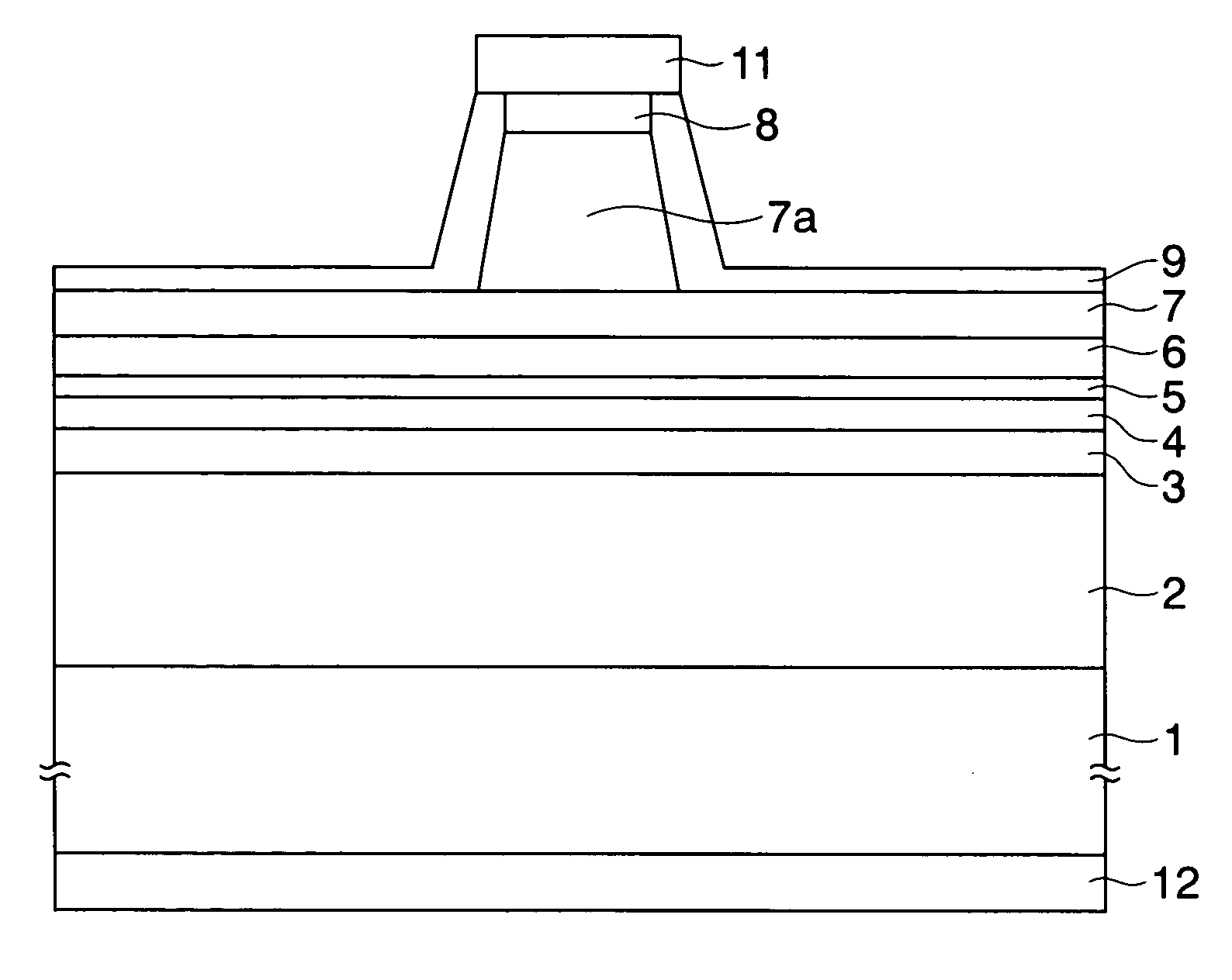
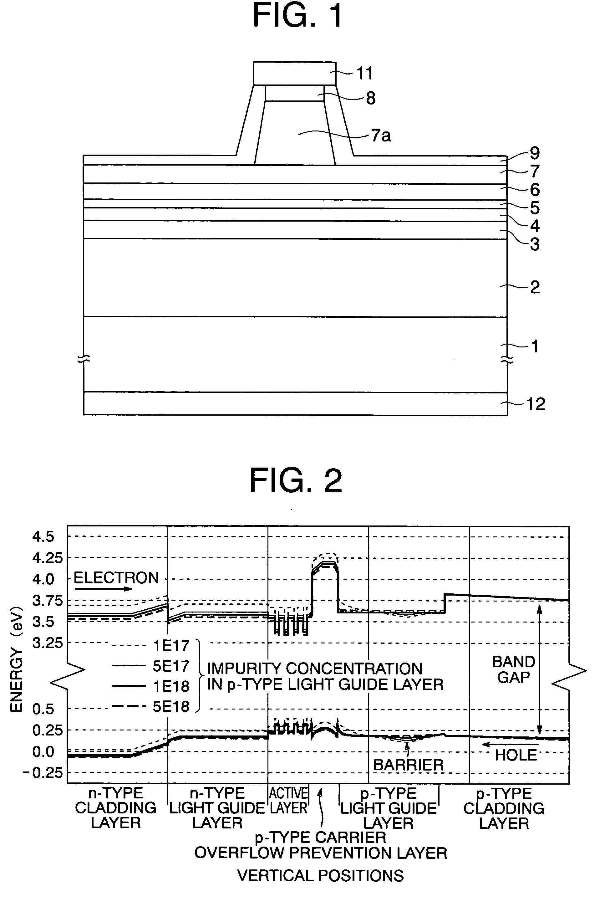
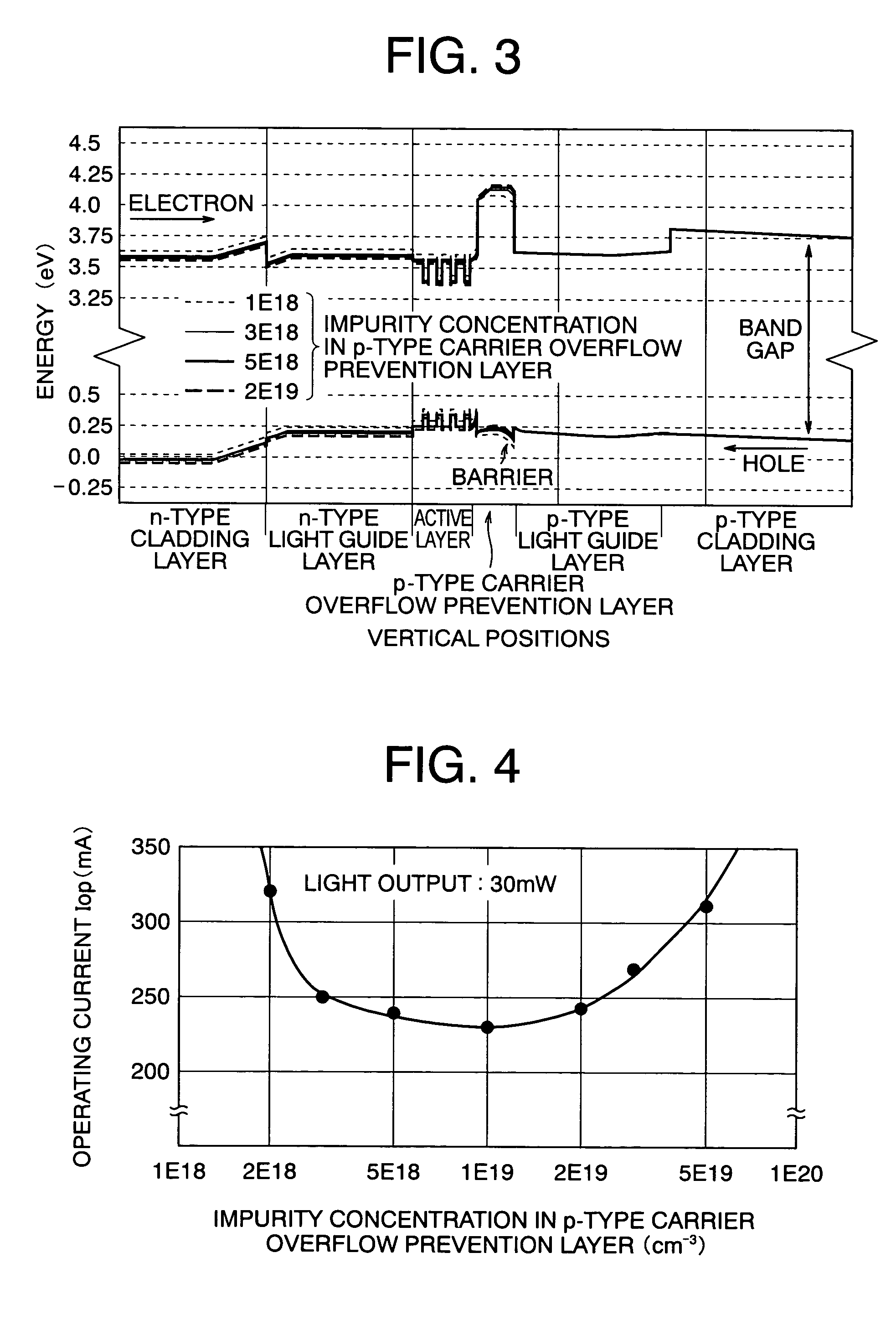
[0022] According to an aspect of the invention, a barrier against a carrier from a p side in a p-type light guide layer disappears substantially by formation of the p-type light guide layer which has an impurity concentration determined to be 1×1018cm−3 or more by doping the impurity. By forming a p-type carrier overflow prevention layer which has an impurity concentration of 5×1018 cm−3 or more and 3×1019 cm−3 or less higher than that in the p-type light guide layer, the barrier against the carrier from the p side in the p-type carrier overflow prevention layer disappears substantially. Therefore, the function of the p-type carrier overflow prevention layer for keeping efficiently the carrier from the n side in the active-layer is maintained as it is, and the c...


PUM


Abstract

Disclosed is a semiconductor light-emitting element, comprising an n-type-cladding layer; a light guide layer positioned on the n-type cladding layer; a multiple quantum well structure active layer positioned on the light guide layer; a p-type carrier overflow prevention layer positioned on the active layer and having an impurity concentration of 5×1018 cm−3 to not more than 3×1019 cm−3; a p-type light guide layer positioned on the p-type carrier overflow prevention layer and-having an impurity concentration of 1×1018 cm−3 or more and less-than that of the p-type carrier overflow prevention layer; and a p-type cladding layer positioned on the p-type light guide layer and having a band gap narrower than the p-type carrier overflow prevention layer, and a method of manufacturing the same.

Description

CROSS REFERENCE TO RELATED APPLICATIONS [0001] This application is based upon and claims the benefit of priority from the prior-Japanese Patent Application No. 2003-296423, filed on Aug. 20, 2003 and Japanese Paten Application No. 2004-227579, filed on Aug. 4, 2004; the entire contents of which are incorporated herein by reference. BACKGROUND [0002] 1. Field of the Invention [0003] The present invention relates-to-a semiconductor light-emitting element which produces light by the recombination of a carrier in a semiconductor and a method of manufacturing the same, and more particularly to a semiconductor light-emitting element suitable for blue light emission and a method of manufacturing the same. [0004] 2. Description of the Related Art [0005] A blue (bluish purple) semiconductor light-emitting element, for example, a 400-nm band semiconductor laser element, adopts a structure having a p-type carrier overflow prevention layer between an active layer and a p-side light guide layer ...

Claims


Application Information

Patent Timeline
Patent Type & Authority Applications(United States)
IPC IPC(8): H01L29/06H01L33/06H01L33/32H01S5/20H01S5/22H01S5/223H01S5/30H01S5/343
CPCB82Y20/00H01S5/2009H01S5/34333H01S5/2231H01S5/3054H01S5/2214
Inventor TANAKA, AKIRAONOMURA, MASAAKI
Owner KK TOSHIBA
Why Eureka
Try Eureka