Method of Fabricating Landing Plug in Semiconductor Device

a technology of semiconductor memory and landing plug, which is applied in the direction of semiconductor memory devices, basic electric elements, electrical equipment, etc., can solve the problems of increasing the number of process steps and the increase of the fabrication cost, and achieve the effect of improving the resistance properties

Inactive Publication Date: 2010-12-30
SK HYNIX INC
View PDF6 Cites 263 Cited by
  • Summary
  • Abstract
  • Description
  • Claims
  • Application Information

AI Technical Summary

Benefits of technology

[0020]In accordance with the invention, by dividing various regions inside a landing plug in a vertical direction upon formation of the landing plug and setting doping concentrations in the re...

Problems solved by technology

However, such a method has the disadvantage that the number of process steps is increased a...

Method used


Image

  • Method of Fabricating Landing Plug in Semiconductor Device
  • Method of Fabricating Landing Plug in Semiconductor Device
  • Method of Fabricating Landing Plug in Semiconductor Device

Examples


Embodiment Construction

[0024]Hereinafter, a method for fabricating a fine pattern in accordance with the invention is described in detail with reference to the accompanying drawings.

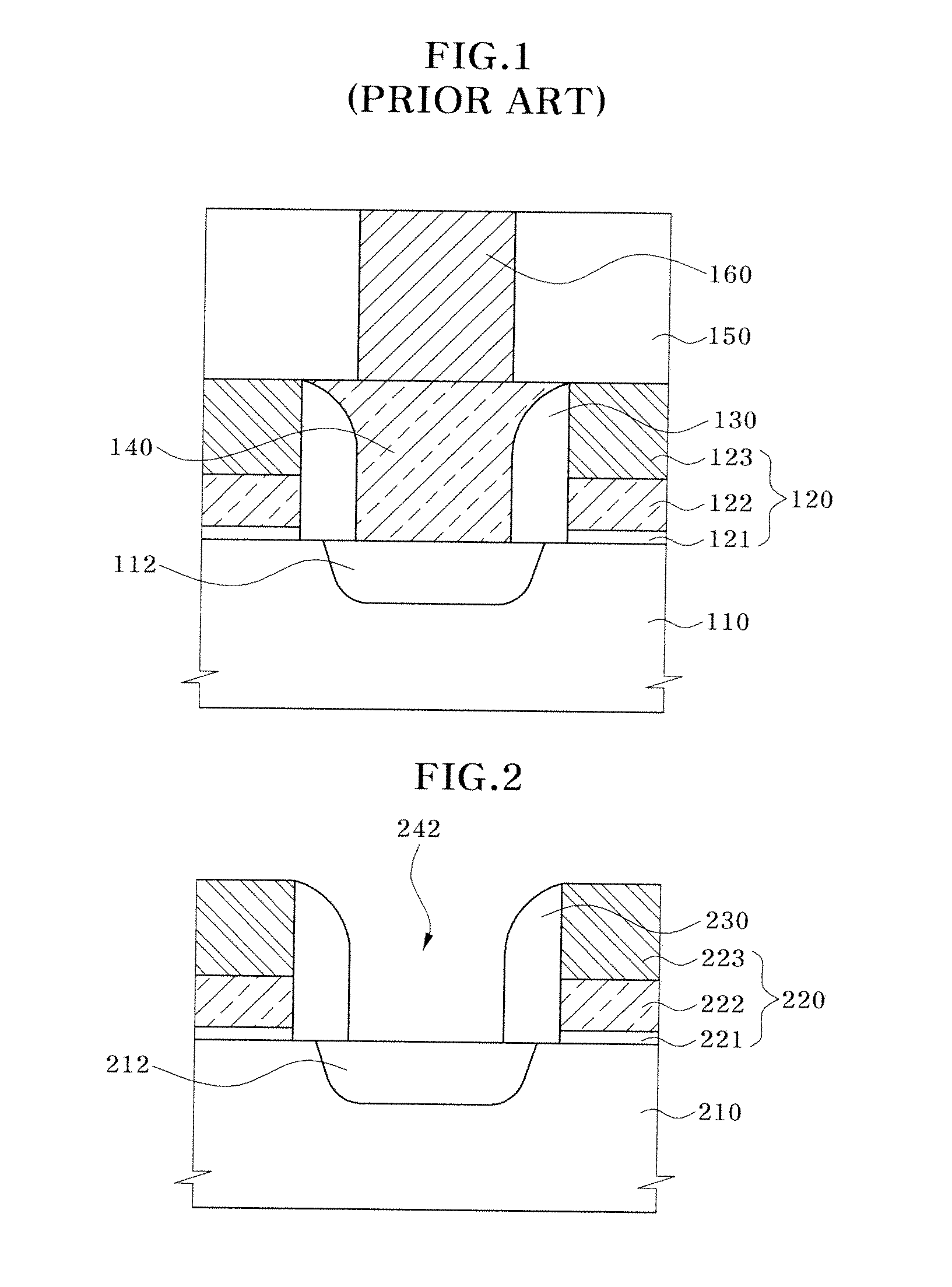
[0025]FIGS. 2 through 7 illustrate a method of fabricating a landing plug in a semiconductor memory device in accordance with one embodiment of the invention.

[0026]Referring first to FIG. 2, a gate stack 220 and an insulating gate spacer layer 230 are formed on a semiconductor substrate 210 having an impurity region 212.

[0027]The impurity region 212 is a source / drain region and is doped with n-type impurity ions or p-type impurity ions. The gate stack structure includes a sequential stack of a gate insulation layer 221, a gate conductive layer 222, and a gate capping layer 223. As such, the gate stack 220 and gate spacer layer 230 are formed, and a landing plug contact hole 242 exposing a surface of the impurity region 212 is formed between adjacent gate spacer layers 230. Though not shown, an insulation layer such as an oxide...


PUM


Abstract

A method of fabricating a landing plug in a semiconductor memory device, which in one embodiment includes forming a landing plug contact hole on a semiconductor substrate having an impurity region to expose the impurity region; forming a landing plug by filling the landing plug contact hole with a polysilicon layer, wherein the landing plug is divided into a first region, a second region, a third region, and a fourth region from a lower portion of the landing plug, and the first region is doped with a first doping concentration that is relatively lowest, the second region is doped with a second doping concentration that is higher than the first doping concentration, the third region is doped with a third doping concentration that is higher than the second doping concentration and the fourth region is not doped; and annealing the resulting product formed with the landing plug.

Description

CROSS-REFERENCE TO RELATED APPLICATION[0001]Priority to Korean patent application number 10-2009-0057629 filed Jun. 26, 2009, the entire disclosure of which is incorporated by reference herein, is claimed.BACKGROUND OF THE INVENTION[0002]The invention relates generally to a semiconductor memory device, and more particularly, to a method of fabricating a landing plug in a semiconductor memory device.[0003]As the degree of integration of semiconductor memory devices has increased, a landing plug is used for electrical connection between an impurity region in a semiconductor substrate and a bit line and a storage node in the case of a Dynamic Random Access Memory (DRAM) device consisting of a transistor and a capacitor. In such a device, a conductive layer is filled in a space adjacent to the impurity region in the semiconductor substrate among spaces between word lines to form a the landing plug and a bit line contact and a storage node contact are formed so as to be connected to the ...

Claims


Application Information

Patent Timeline
IPC IPC(8): H01L21/768
CPCH01L21/28525H01L27/10855H01L21/76895H01L21/28556Y10S438/923H10B12/0335H01L21/28H10B99/00H10B12/00
Inventor ROUH, KYOUNG BONG
Owner SK HYNIX INC
Why Eureka
Try Eureka