
Semiconductor processing apparatus with a ceramic-comprising surface which exhibits fracture toughness and halogen plasma resistance

Active Publication Date: 2015-05-28
APPLIED MATERIALS INC
View PDF18 Cites 18 Cited by
  • Summary
  • Abstract
  • Description
  • Claims
  • Application Information

AI Technical Summary

Benefits of technology

The patent text discusses the problem of erosion (erosion rate) in semiconductor processing apparatus caused by the exposure of surfaces to chemical reagents and plasma ions. The text describes the use of ceramic materials, such as yttrium oxide and zirconium oxide, as protective coatings to reduce erosion. However, these materials have decreased mechanical properties. The patent proposes a solution by adding zirconium oxide powder to yttrium oxide powder to create a solid solution with improved plasma resistance and mechanical properties. The combination of powders is compacted and sintered to form a single phase or two phase solid solution with excellent plasma erosion resistance and improved mechanical properties compared to previously known solid solutions.

Problems solved by technology

Plasmas used for plasma-enhanced chemical vapor deposition processes often tend to be corrosive as well.
However, the integrity of the anodization layer may be deteriorated by impurities in the aluminum or aluminum alloy, so that corrosion begins to occur early, shortening the life span of the protective coating.
However, current materials used for protective layers deteriorate over time and eventually leave the aluminum alloy subject to attack by the plasma, even though the life span of the protective layer is extended over that of anodized aluminum.
However, due to the concentration of reactive species which are present at the surface of the gas distribution plate, the lifetime of the gas distribution plate has typically been limited, from about 8 processing days to about 80 processing days, depending on the corrosivity of the plasma created in the processing chamber.
This translates to low costs of manufacturing, reduced wafer defects, increased lifetime, and increased mean time between cleaning.
However, the plasma resistance properties of these ceramic materials is not adequate in many instances, particularly when a fluorine plasma source gas is involved.
The recent introduction of Y2O3 ceramic shows improved plasma resistance properties, but this material generally exhibits weak mechanical properties that limits its applications for general use in semiconductor processing components, processing kits, and chamber liners.
A protective material may be applied as a coating over the apparatus surface; however, this may not be the best solution to avoiding erosion.
The coating is constantly getting thinner (eroding) during a plasma etch, and there is an increased risk that the substrate beneath the coating will be attacked by the plasma penetrating the coating layer.
However, frequently the materials which are more erosion-resistant are more crystalline, and an improvement in erosion resistance comes at a cost, in the form of decreased mechanical properties (such as ductility) of the apparatus.

Method used


Image

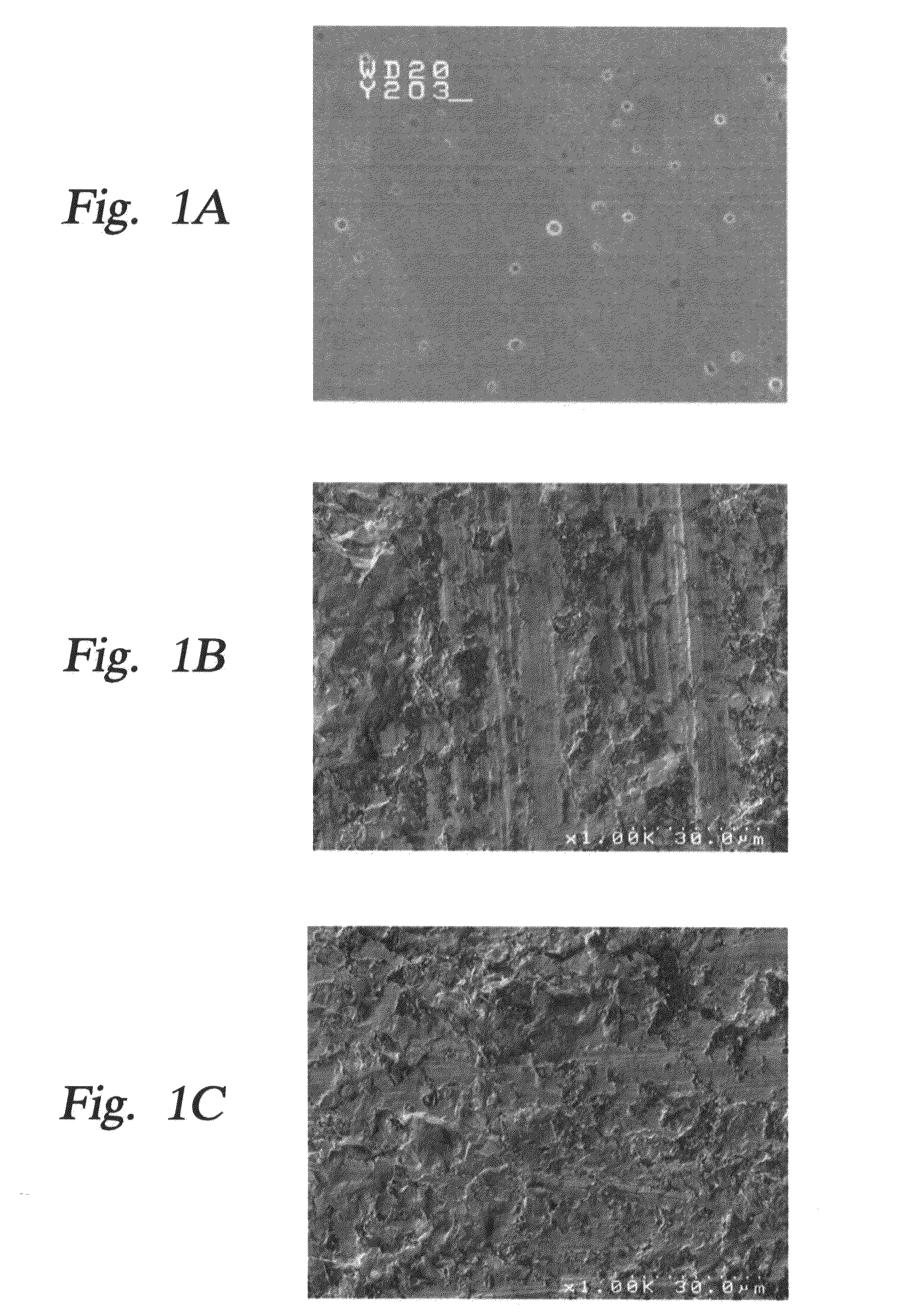
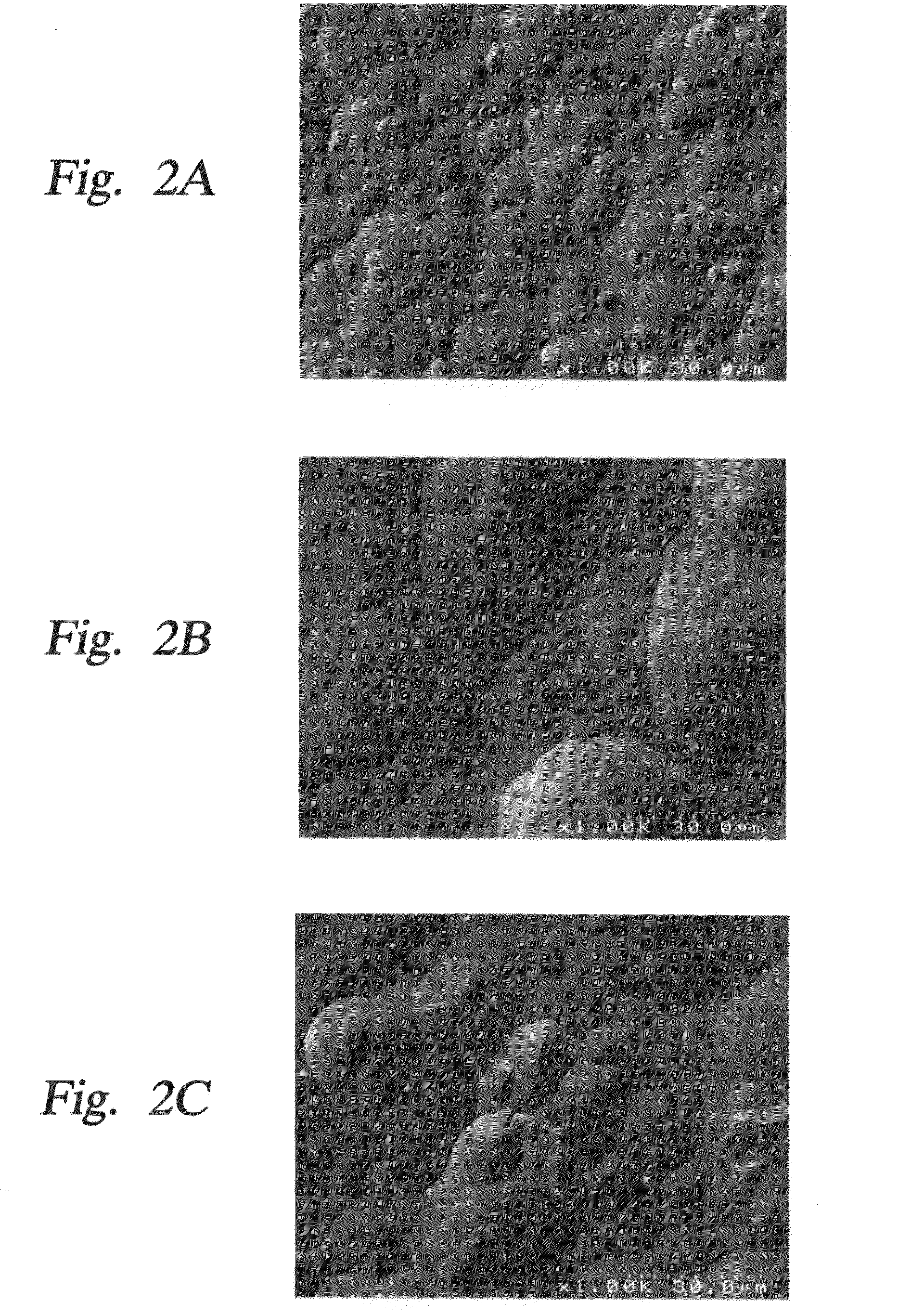
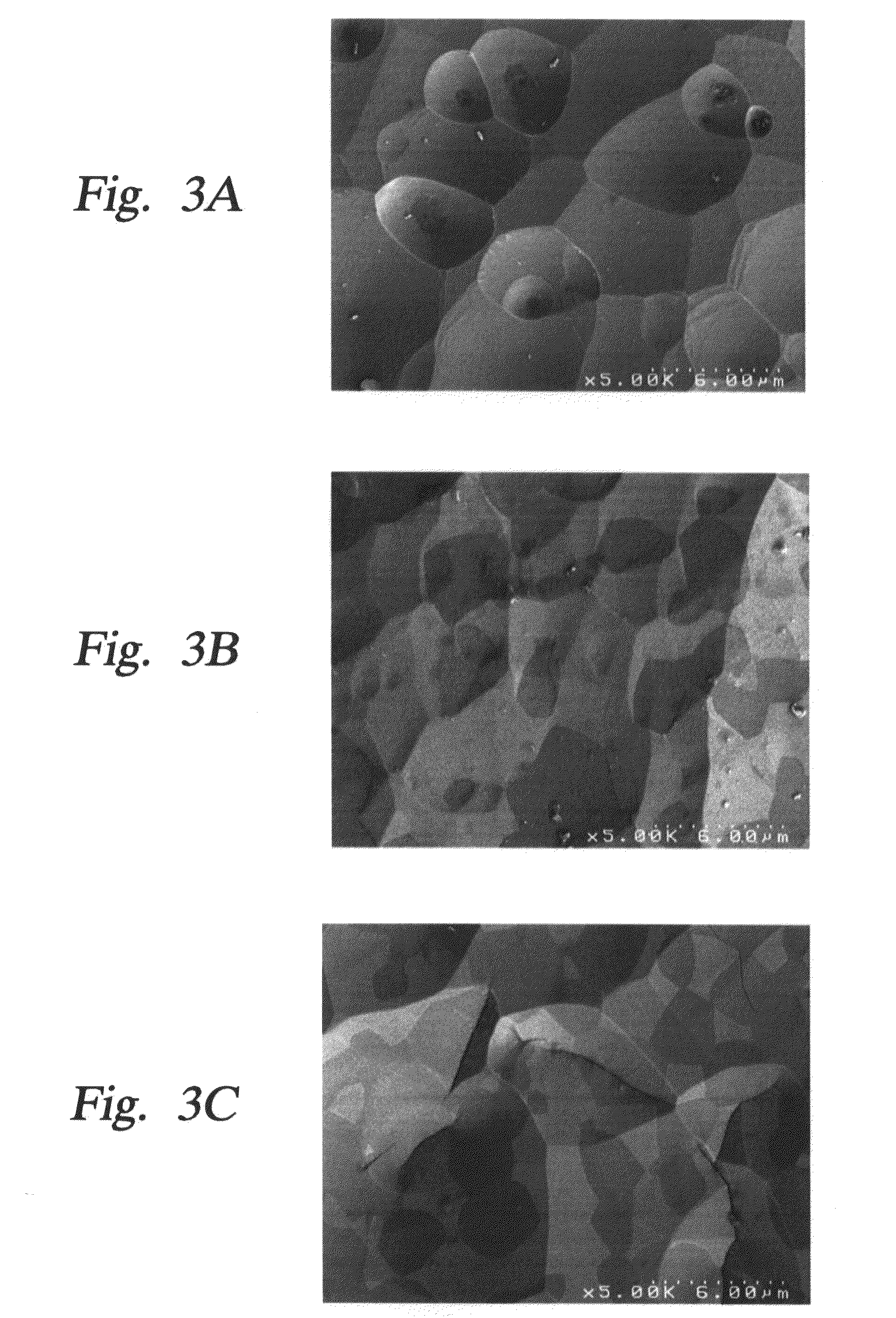
  • Semiconductor processing apparatus with a ceramic-comprising surface which exhibits fracture toughness and halogen plasma resistance
  • Semiconductor processing apparatus with a ceramic-comprising surface which exhibits fracture toughness and halogen plasma resistance
  • Semiconductor processing apparatus with a ceramic-comprising surface which exhibits fracture toughness and halogen plasma resistance

Examples


example embodiments

Example One

Etch Plasma Process Conditions for Erosion Rate Testing

[0044]Tables One-Three, below, provides the etch plasma compositions and etch plasma processing conditions which were used for evaluation of a series of test coupon materials. There were three basic different sets of etch plasma conditions which were used for the erosion rate testing: 1) Trench etching, where the etch plasma source gas and etch process conditions were representative of etching a trench feature size beyond 65 nm technology, i.e. smaller than 65 nm, into a multilayered semiconductor substrate. Such a substrate typically includes an antireflective coating (ARC or BARC) layer, an organic or inorganic dielectric layer, a metal layer, and an etch stop layer. Contact Via etching, where the etch plasma source gas and etch process conditions were representative of etching a contact via having an aspect ratio of about 30 in production and 40 plus in the developed device substrate, and having a diameter of beyon...

example two

Comparative Relative Erosion Rates of Various Ceramic Materials Compared with Aluminum Oxide

[0046]Aluminum oxide has frequently been used as a protective layer or liner when a semiconductor process makes use of an etchant plasma. Using aluminum oxide as the base comparative material, we determined the relative etch rates, in a Trench Etch (CF4 / CHF3) environment. With aluminum oxide having a relative erosion rate of 1, we found that the relative erosion rate of quartz was about 2.2 times that of aluminum oxide. The relative erosion rate of silicon carbide was about 1.6 times that of aluminum oxide. The relative erosion rate of zirconia was about 0.8 times that of aluminum oxide. The relative erosion rate of pure yttrium oxide was about 0.19 times that of aluminum oxide. The relative erosion rate of a yttrium oxide, zirconium oxide, aluminum oxide ceramic composite, formed from 55 mole % yttrium oxide, 20 mole % zirconium oxide, and 25 mole % aluminum oxide was about 0.2 times that of...

example three

Measured Erosion Rates for Trench Etching Process

[0047]With reference to the trench etching method described above, the sample substrate test coupon erosion rates measured were as follows. The erosion rate of aluminum oxide was 1.1 μm / hr. The erosion rate of bulk yttrium oxide was 0.3 μm / hr. The erosion rate of a the a yttrium oxide, zirconium oxide, aluminum oxide ceramic composite, formed from 55 mole % yttrium oxide, 20 mole % zirconium oxide, and 25 mole % aluminum oxide was 0.1 μm / hr. The erosion rate of a yttrium oxide, zirconium oxide, aluminum oxide ceramic composite, formed from 63 mole % yttrium oxide, 23 mole % zirconium oxide, and 14 mole % aluminum oxide was 0.07 μm / hr.


PUM


Abstract

A solid solution-comprising ceramic article useful in semiconductor processing, which article may be in the form of a solid, bulk ceramic, or may be in the form of a substrate having a ceramic coating of the same composition as the bulk ceramic material on at least one outer surface. The ceramic article is resistant to erosion by halogen-containing plasmas and provides advantageous mechanical properties. The solid solution-comprising ceramic article is formed from a combination of yttrium oxide and zirconium oxide. The ceramic-comprising article includes ceramic which is formed from zirconium oxide at a molar concentration ranging from about 96 mole % to about 91 mole %, and yttrium oxide at a molar concentration ranging from about 4 mole % to about 9 mole %.

Description

[0001]This application is a divisional application of U.S. application Ser. No. 13 / 199,521, entitled “Semiconductor Processing Apparatus Comprising A Coating Formed From a Solid Solution of Yttrium Oxide and Zirconium Oxide”, filed Aug. 31, 2011, which has been allowed; which is a divisional application of U.S. application Ser. No. 12 / 660,068, entitled “Semiconductor Processing Apparatus Which Is Formed From Yttrium Oxide and Zirconium Oxide to Produce a Solid Solution Ceramic Apparatus”, which issued as U.S. Pat. No. 8,034,734 on Oct. 11, 2011; which is a continuation application of U.S. application Ser. No. 11 / 796,210, entitled “Method of Reducing the Erosion Rate of Semiconductor Processing Apparatus Exposed to Halogen-Containing Plasmas”, which has gone abandoned.[0002]The present application is related to a series of applications filed by various inventors of the present application, many of the applications relate to the use of a yttrium-oxide comprising ceramic in the form of...

Claims


Application Information

Patent Timeline
IPC IPC(8): H01L21/67
CPCH01L21/67011C04B35/486C04B35/505C04B2235/3217C04B2235/3225C04B2235/3244C04B2235/77C04B2235/785C04B2235/786C04B2235/80C04B2235/96C04B2235/9607C04B2235/9669
Inventor SUN, JENNIFER Y.DUAN, REN-GUANYUAN, JIEXU, LICOLLINS, KENNETH S.
Owner APPLIED MATERIALS INC
Learn More