Wiring layer structure and process for manufacture thereof

a layer structure and wire technology, applied in the direction of cable/conductor manufacturing, semiconductor/solid-state device details, transistors, etc., can solve the problems of reducing the adhesion property unstable dangle bonds, and affecting the adhesion of cu to the underlying substrate material, so as to improve the adhesion property and prevent diffusion. , the effect of excellent diffusion barrier property

Active Publication Date: 2012-03-22
MITSUBISHI MATERIALS CORP +1
View PDF4 Cites 9 Cited by
  • Summary
  • Abstract
  • Description
  • Claims
  • Application Information

AI Technical Summary

Benefits of technology

[0035]As described above, in accordance with the present invention, the oxide layer containing at least one of Al, Zr, and Ti is formed in the interface between the Cu alloy layer and either of the oxygen-containing Cu layer or the Cu alloy layer. Thereby, it is possible to provide a wiring layer structure which has a high adhesion property to the underlying substrate, excellent diffusion barrier property to prevent diffusion to the underlying substrate, excellent hydrogen plasma resistance (resistance to hydrogen plasma), and a low electrical resistance, and a manufacturing method thereof.

Problems solved by technology

However, there are problems in that Cu is inferior in an adhesion property to underlying substrate materials such as glass, Si, and the like, compared to adhesion properties of wiring materials such as Al and the like, and Cu is diffused to an underlying substrate.
It is known that in the case where the above-mentioned Cu wiring layer pattern is formed on a non-single crystal semiconductor thin film such as an amorphous silicon thin film or a polycrystalline silicon thin film and a portion of the semiconductor thin film is exposed, a large number of dangling bonds (bonding partners which are not involved in a bond due to losing their covalent bonding partners) exist in the surface of the exposed semiconductor thin film The dangling bonds are unstable.
As a result, the layer is peeled off at the interface and the adhesion property is deteriorated (see, for example, Non-Patent Document 2).

Method used


Image

  • Wiring layer structure and process for manufacture thereof
  • Wiring layer structure and process for manufacture thereof
  • Wiring layer structure and process for manufacture thereof

Examples


examples

[0090]Wiring layer structures were formed in reality on the basis of the present invention, and the wiring layer structures were evaluated. Hereinafter, the evaluation results will be described.

[0091]At first, a glass substrate having dimensions of 320 mm long, 400 mm wide, and 0.7 mm thick was prepared of which the surface was coated with an amorphous Si layer.

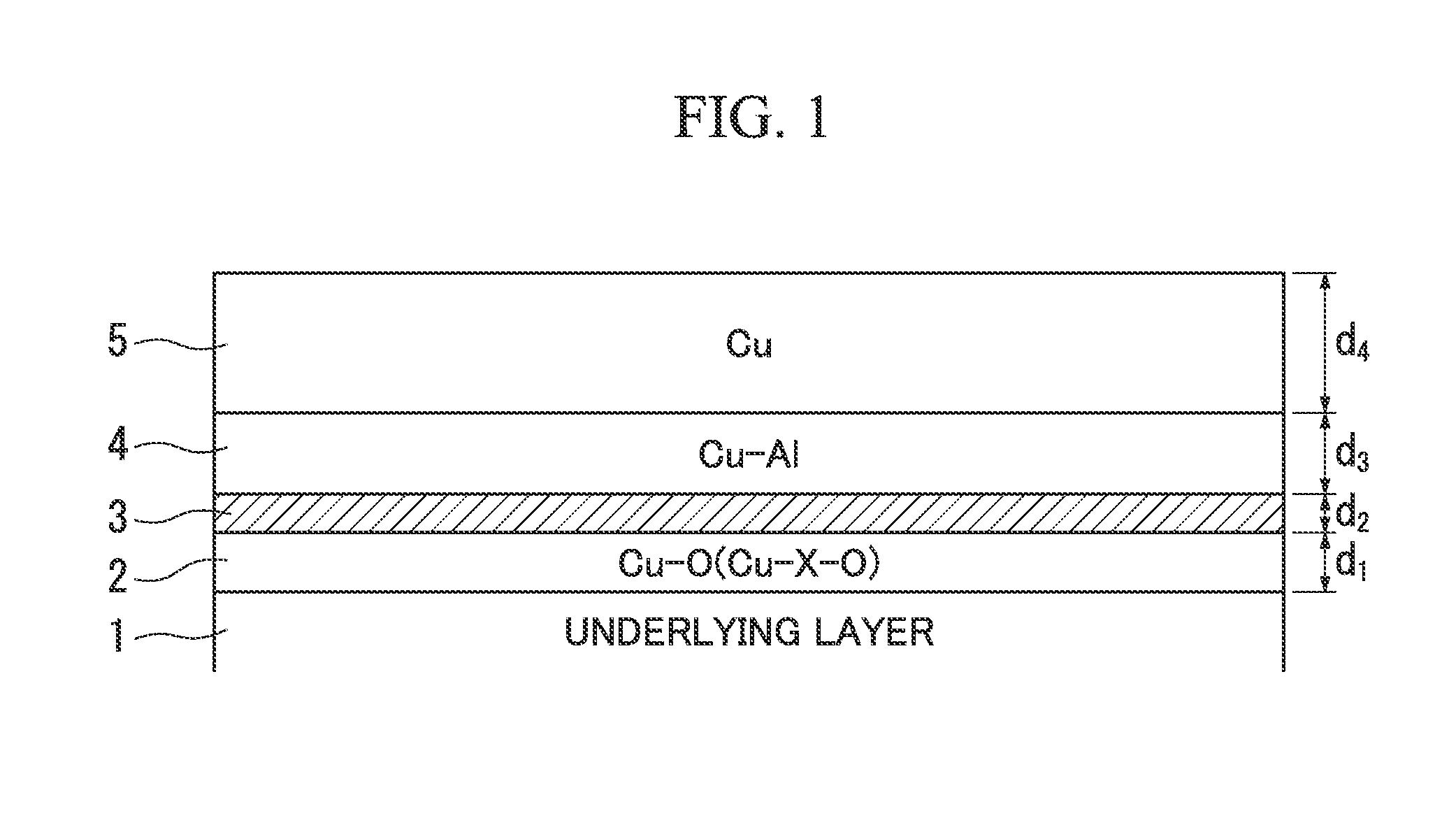
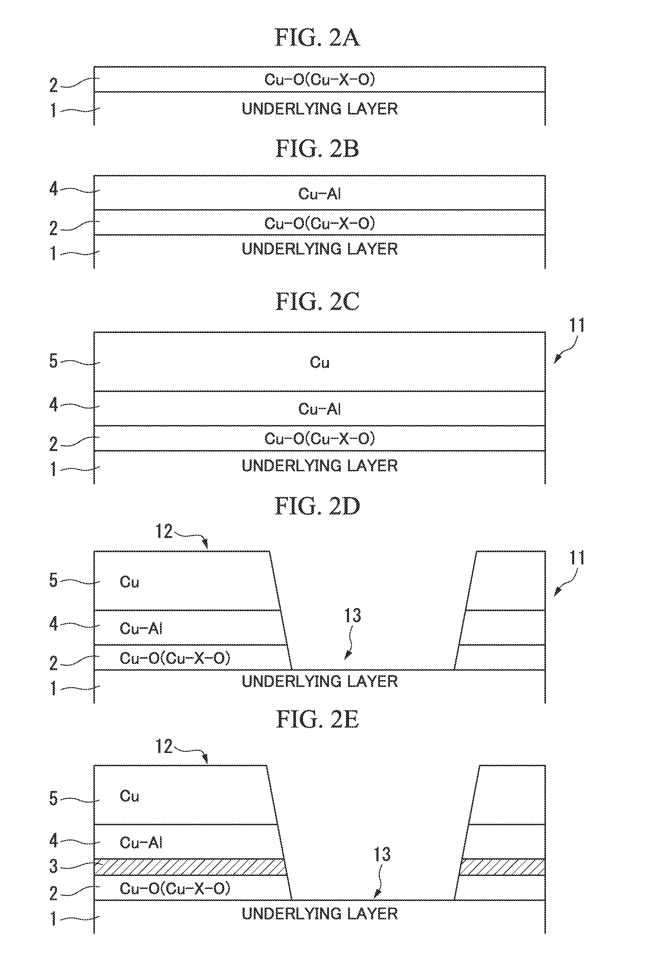
[0092](Preparation of Oxygen-Containing Cu Alloy Layer)

[0093]Next, a Cu alloy sputtering target was prepared by melting and adjusting the composition to include Cu-4atom % Al (melting adjustment). The glass substrate was loaded in a sputtering apparatus, and sputtering was performed using the Cu alloy sputtering targets under the following conditions to form an oxygen-containing Cu alloy layer having a thickness of 50 nm:

[0094]Atmosphere: oxidizing atmosphere of Ar+oxygen (Ar / oxygen=90 / 10 by vol %);

[0095]Pressure of the atmosphere: 0.4 Pa; and

[0096]Substrate heating temperature: 100° C.

[0097](Preparation of Cu Alloy Layer)

[00...


PUM

PropertyMeasurementUnit
thicknessaaaaaaaaaa
thicknessaaaaaaaaaa
thicknessaaaaaaaaaa

Abstract

This wiring layer structure includes: an underlying substrate of a semiconductor substrate or a glass substrate; an oxygen-containing Cu layer or an oxygen-containing Cu alloy layer which is formed on the underlying substrate; an oxide layer containing at least one of Al, Zr, and Ti which is formed on the oxygen-containing Cu layer or the oxygen-containing Cu alloy layer; and a Cu alloy layer containing at least one of Al, Zr, and Ti which is formed on the oxide layer.

Description

TECHNICAL FIELD[0001]The present invention relates to a wiring layer structure. In particular, the present invention relates to a wiring layer structure used in a semiconductor device such as a transistor and the like and a method for manufacturing the wiring layer structure.[0002]The present application claims priority on Japanese Patent Application No. 2009-141440 filed on Jun. 12, 2009, the content of which is incorporated herein by reference.BACKGROUND ART[0003]From the viewpoint of high-speed driving and reduction in cost, expectations have been focused on a Cu-based wiring layer having a lower resistivity than that of an Al-based wiring layer which is the mainstream of a wiring layer for a TFT panel at present.[0004]However, there are problems in that Cu is inferior in an adhesion property to underlying substrate materials such as glass, Si, and the like, compared to adhesion properties of wiring materials such as Al and the like, and Cu is diffused to an underlying substrate....

Claims


Application Information

Patent Timeline
Patent Type & Authority Applications(United States)
IPC IPC(8): H01L29/786H05K3/06H01L21/04H01L29/40H01L21/768
CPCC22C9/00C22C9/01H01L23/53238H01L29/45H01L27/124H01L2924/0002H01L29/4908H01L2924/00H01L21/2855
Inventor MAKI, KAZUNARIYAGUCHI, KENICHINAKASATO, YOSUKE
Owner MITSUBISHI MATERIALS CORP
Why Eureka
Try Eureka