Plasma processing apparatus and method

A plasma and processing device technology, which is applied in the fields of plasma, semiconductor/solid-state device manufacturing, gaseous chemical plating, etc., can solve the problem of not fully ensuring the etching selectivity ratio of Low-k film and SiC layer, etc.

Active Publication Date: 2007-06-20
TOKYO ELECTRON LTD
View PDF5 Cites 11 Cited by
  • Summary
  • Abstract
  • Description
  • Claims
  • Application Information

AI Technical Summary

Problems solved by technology

However, plasma etching using the fluorocarbon-based processing gas described in Patent Document 2 and Patent Document 3 cannot sufficiently ensure the etching selectivity ratio between the Low-k film and the SiC layer.

Method used


Image

  • Plasma processing apparatus and method
  • Plasma processing apparatus and method
  • Plasma processing apparatus and method

Examples


Embodiment approach 1

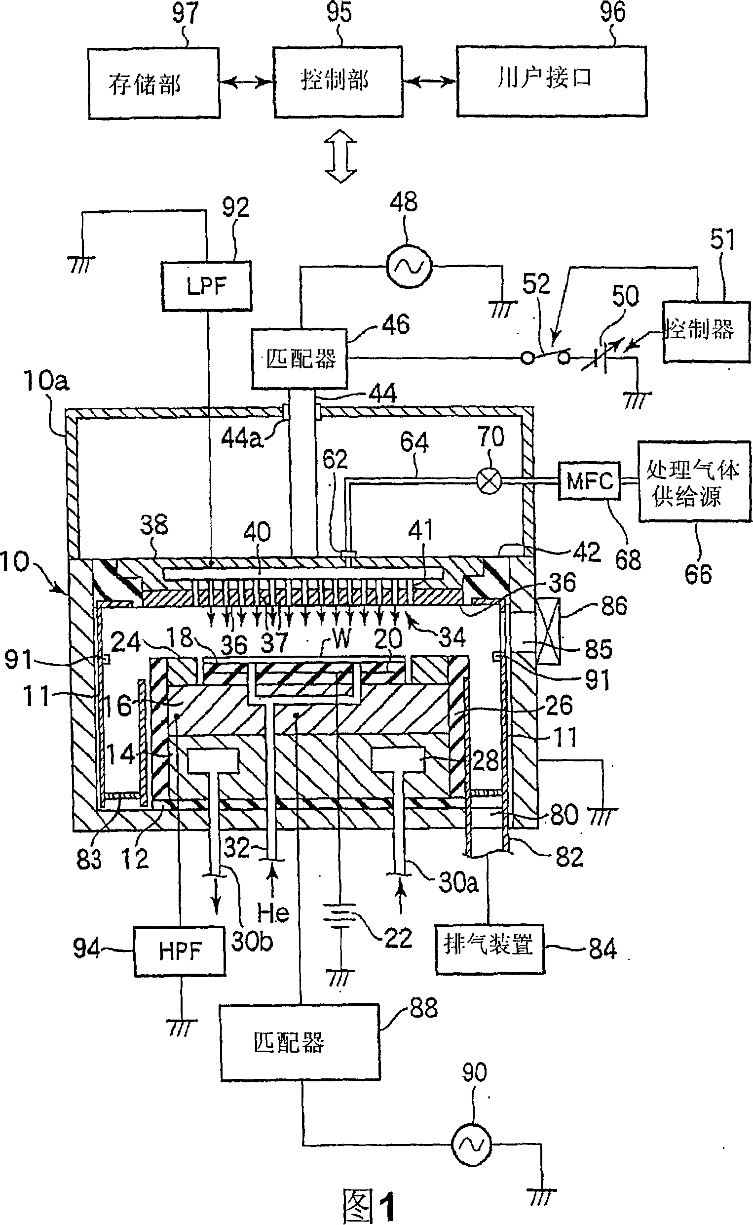
[0213] First, the first embodiment will be described. FIG. 1 is a schematic cross-sectional view showing a plasma etching apparatus according to a first embodiment of the present invention.

[0214] This plasma etching apparatus is configured as a capacitively coupled parallel plate plasma etching apparatus, and has a substantially cylindrical chamber (processing container) 10 made of, for example, aluminum whose surface is anodized. The chamber 10 is safety grounded.

[0215] At the bottom of the chamber 10 , a cylindrical susceptor support 14 is arranged via an insulating plate 12 made of ceramics or the like, and a susceptor 16 made of, for example, aluminum is provided on the susceptor support 14 . The susceptor 16 constitutes a lower electrode, and a semiconductor wafer W serving as a substrate to be processed is placed thereon.

[0216] An electrostatic chuck 18 that attracts and holds the semiconductor wafer W by electrostatic force is provided on the upper surface of...

Embodiment approach 2

[0362] Next, a second embodiment of the present invention will be described.

[0363] 34 is a schematic cross-sectional view showing a plasma etching apparatus according to a second embodiment of the present invention. In FIG. 34, the same components as those in FIG. 1 are denoted by the same reference numerals, and description thereof will be omitted.

[0364]In this embodiment, instead of the upper electrode 34 of the first embodiment, an upper electrode 34' having the following structure is provided. The upper electrode 34' is composed of a ring-shaped outer upper electrode 34a disposed opposite to the susceptor 16 at a predetermined interval, and a disk-shaped inner upper electrode 34b disposed radially inward of the outer upper electrode 34a in an insulated state. constitute. These are involved in the generation of plasma, and have a relationship in which the outer upper electrode 34 a is the main one and the inner upper electrode 34 b is the auxiliary one.

[0365] As...

no. 3 approach

[0408] In the third embodiment, components common to those in the first and second embodiments are denoted by the same symbols.

[0409] 40 is a schematic cross-sectional view showing a plasma etching apparatus according to a third embodiment of the present invention.

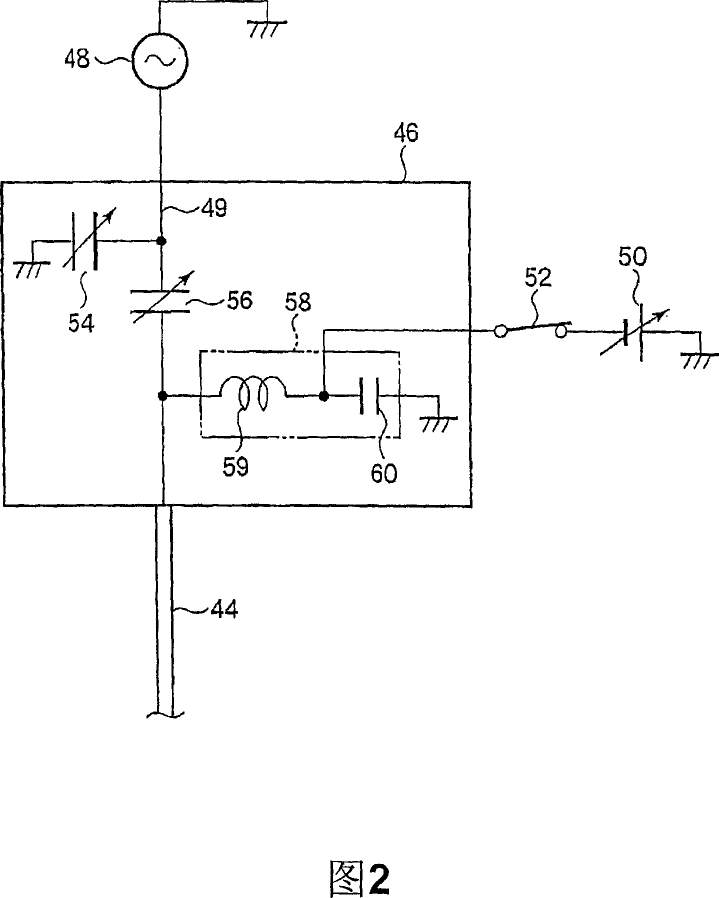
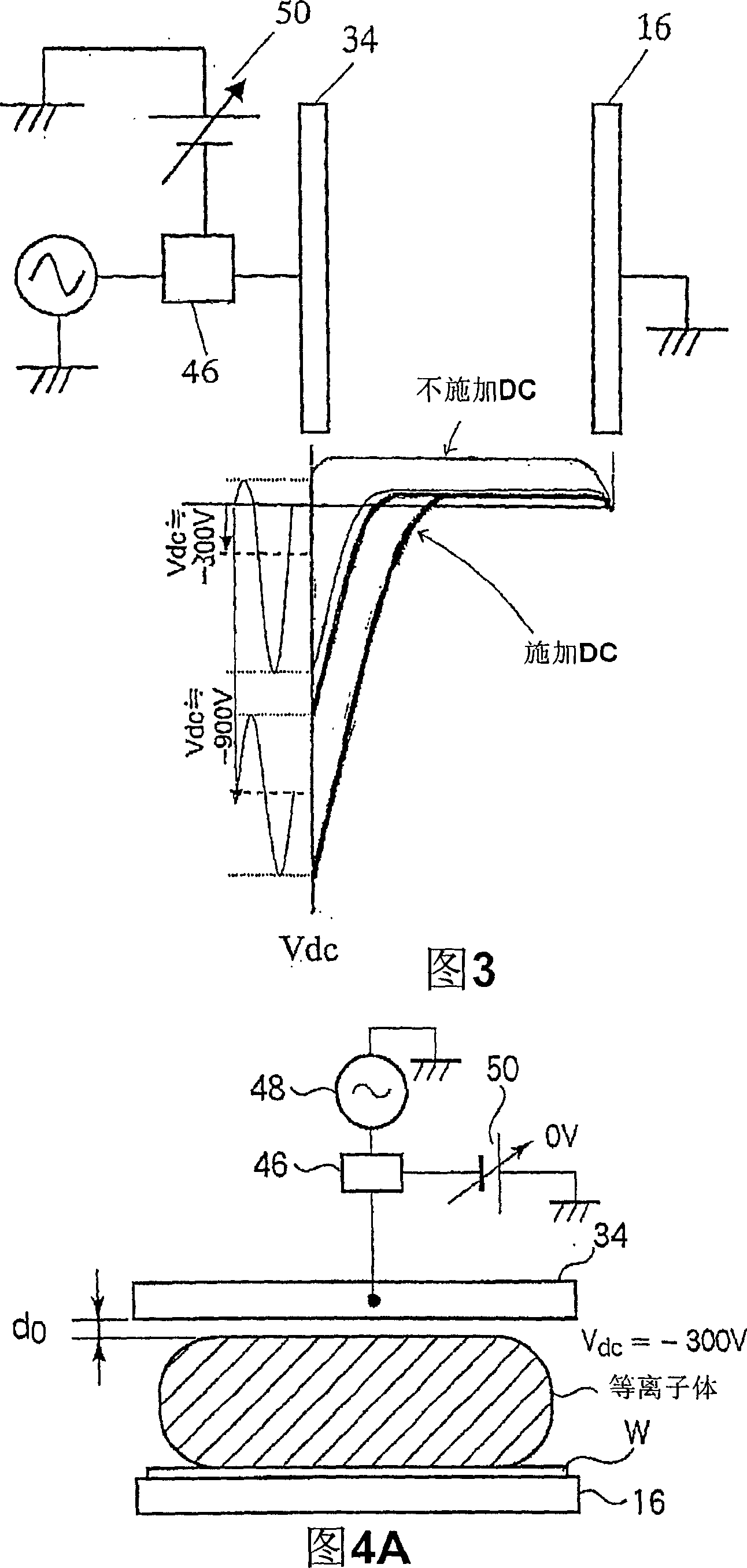
[0410] That is, it applies high-frequency (RF) power of, for example, 40 MHz for plasma generation from the first high-frequency power supply 88 to the susceptor 16 as the lower electrode, and supplies the susceptor 16 as the lower electrode from the second high-frequency power supply 90 . 16. A lower RF dual-frequency application type plasma etching apparatus for applying high-frequency (RF) power of, for example, 2 MHz for ion introduction. As shown in the figure, a variable DC power supply 50 is connected to the upper electrode 34 to apply Plasma etching apparatus with specified direct current (DC) voltage. This plasma etching apparatus will be described in detail using FIG. 41 .

[0411] This plasma etchi...


PUM

PropertyMeasurementUnit
relative permittivityaaaaaaaaaa

Abstract

The invention provides a plasma processing system characterised in that comprises a processing container for receiving a substrate to be processed and performing vacuum exhausting air; a first electrode and a second electrode supporting the substrate to be processed arranged in the processing container oppositely; a first high-frequency power supply unit for applying a first high-frequency power of relatively high frequency to the second electrode; a second high-frequency power supply unit for applying a second high-frequency power of relatively low frequency to the second electrode; a DC power supply for applying a DC voltage to the first electrode; a gas supply unit for supplying gas which is to be processed to the processing container; and a controlling device for controlling one of the applied voltage, the applied current and the applied power from the DC power supply to the first electrode.

Description

[0001] This case is filed on June 21, 2005 , the application number is 200580020518.0 (PCT / JP2005 / 011333) , the name of the invention is Plasma treatment apparatus and method divisional application of the patent application. technical field [0002] The present invention relates to a plasma processing device, a plasma processing method, and a computer-readable storage medium for performing plasma processing on substrates to be processed such as semiconductor substrates. Background technique [0003] For example, in the manufacturing process of a semiconductor device, in order to form a predetermined pattern on a predetermined layer formed on a semiconductor wafer as a substrate to be processed, a plasma etching process using a resist as a mask and etching with plasma is often used. [0004] As a plasma etching apparatus for performing such plasma etching, various apparatuses are used, and a capacitive coupling type parallel plate plasma processing apparatus is mainly us...

Claims


Application Information

Patent Timeline
Patent Type & Authority Applications(China)
IPC IPC(8): H05H1/24H05H1/02H01L21/306C23C16/00C23F1/00
Inventor 舆石公日向邦彦大谷龙二松本直树矢野大介速水利泰杉本胜小林典之吉备和雄大矢欣伸山泽阳平山崎广树舆水地盐齐藤昌司岩田学花冈秀敏佐藤学
Owner TOKYO ELECTRON LTD
Why Eureka
Try Eureka