Optical waveguide and method for producing same

a technology of optical waveguides and optical fibers, applied in the field of optical waveguides, can solve the problems of device complexity, cost versus effect, and not yet spread, and achieve the effect of ensuring high light propagation characteristics

Inactive Publication Date: 2005-05-12
SONY CORP
View PDF8 Cites 22 Cited by
  • Summary
  • Abstract
  • Description
  • Claims
  • Application Information

AI Technical Summary

Benefits of technology

[0016] An object of the present invention is to provide an optical waveguide having an optical waveguide path capable of secu

Problems solved by technology

Recently, although optical fiber channels and optical data links and other technology for using optical transmission have begun spreading in use, at the present time they have not yet spread to an extent of the optical communications and transmitting means replacing wired communications and transmitting means.
One of the reasons for this is the issue of cost versus effect.
Specifically, for example, there can be mentioned the points that, in order to maintain the performance of optical communications (for example, transmission rate and transmission quality), technology is required for precise positioning between a light emitting element and a light receiving element constituting the optical communications device and the optical fiber, that countermeasures for light leakage, consideration of electromagnetic interference, and countermeasures to noise are necessary, and that, as a result, the device becomes complex and expensive etc.
Accordingly, the issues have arisen of how to deal with the rise in the frequency of the signal processing clocks, the rise in the degree of parallel operation, and the rise in the speed of the access to the memories.
In memory access circuits and processors of multi-microprocessor (MPU) configurations, however, the parasitic capacitance component of the portion which becomes necessary at the time of mounting, for example, the package of the semiconductor device, is large, so high speed signal transmission operation becomes difficult in the electric wiring connected to the outside of the semiconductor chips.
Further, application of a high speed signal to the electric wiring can cause spikes in the current or the voltage and can cause electromagnetic interference (EMI) and other types of electromagnetic interference noise, reflection noise, and crosstalk no

Method used


Image

  • Optical waveguide and method for producing same
  • Optical waveguide and method for producing same
  • Optical waveguide and method for producing same

Examples


first embodiment

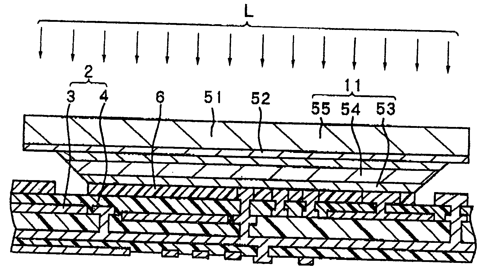
[0117] First, an explanation will be made of the configuration of an optical waveguide according to a first embodiment of the present invention with reference to FIG. 1.

[0118]FIG. 1 is a view showing the sectional configuration of an optical waveguide 1 according to the present embodiment. This optical waveguide 1 is provided with a multilayer circuit board 2, an optical waveguide path 11 bonded to the multilayer circuit board 2 via a bonding layer 6, a light receiving element 21 mounted on the multilayer circuit board 2 over the optical waveguide path 11 as a spacer, IC chips 25 and 35, and a light emitting element 31. Here, the multilayer circuit board 2 corresponds to a concrete example of the “substrate” and “second substrate” of the present invention. Further, the IC chips 25 and 35 correspond to concrete examples of the “integrated circuit” of the present invention.

[0119] The multilayer circuit board 2 is an electric circuit substrate comprised of a plurality of electrical w...

second embodiment

[0152] The second embodiment relates to a method for producing the optical waveguide. The optical waveguide covered by this method is similar to that of the first embodiment except for the point that the optical waveguide paths are spaced from each other. Below, an explanation will be made of the method for producing the optical waveguide of the present embodiment by referring to FIG. 1 through FIGS. 5A and 5B and FIG. 13 through FIG. 20. FIG. 13 through FIG. 20 are partially cutaway perspective views representing steps of production. Note that constituent elements the same as those of the first embodiment are given the same reference numerals and detailed explanations thereof are omitted.

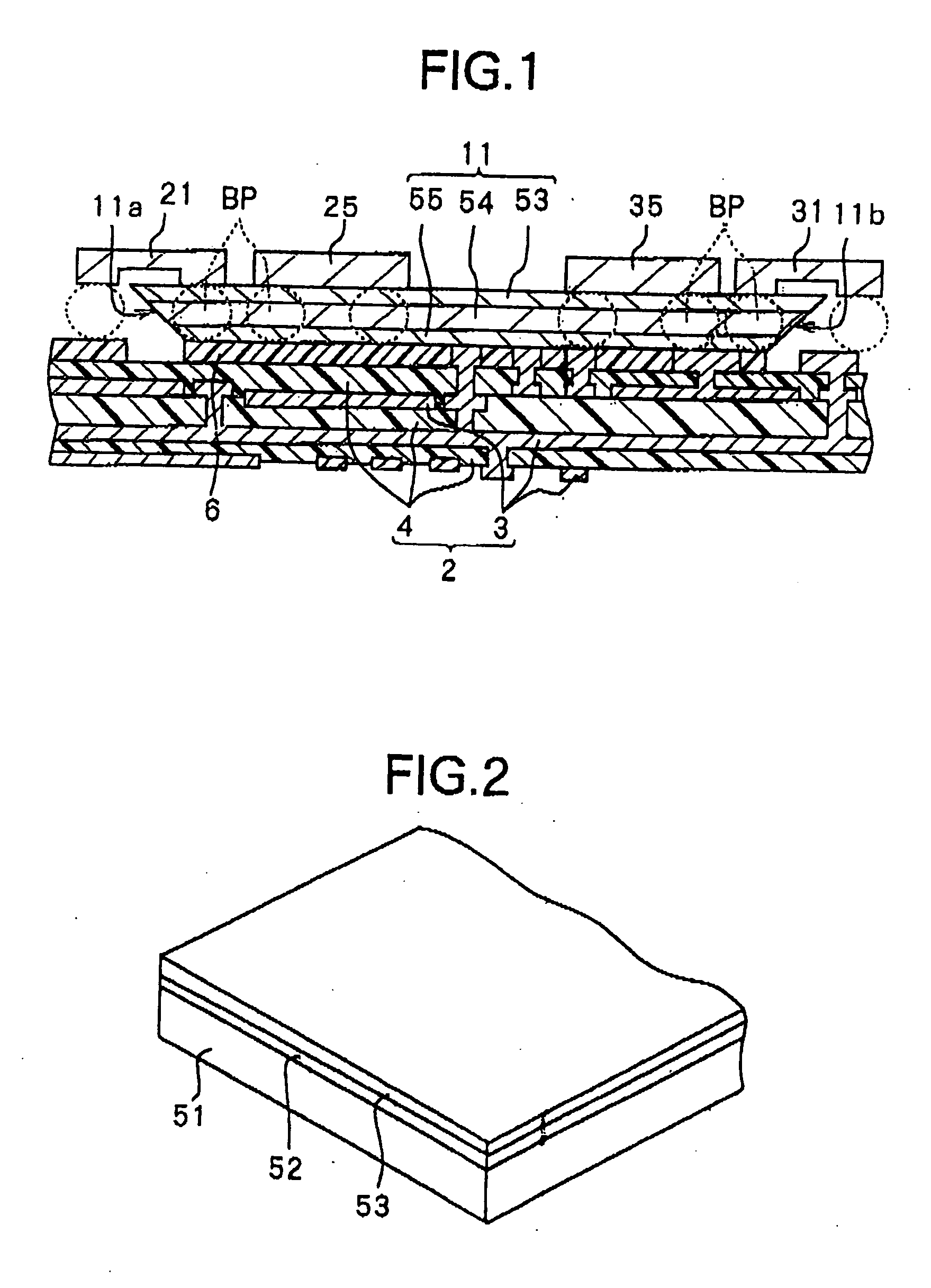
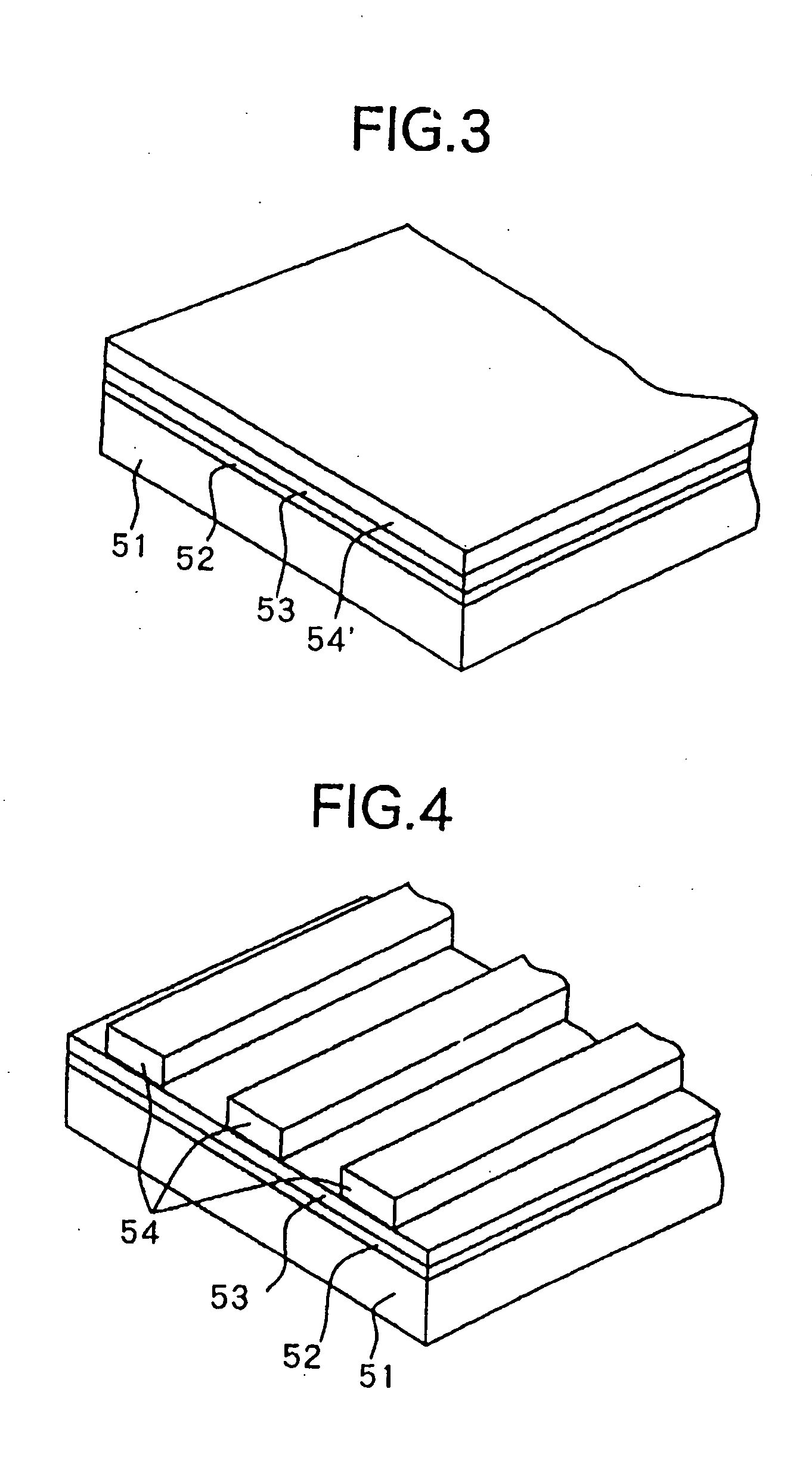
[0153] In the method of production according to the present embodiment, first, in the same way as the steps of productions shown in FIG. 2 to FIGS. 5A to 5B of the first embodiment, the substrate separation layer 52 and the optical waveguide path 11 are formed on a transparent substrate 51.

[0154]...

third embodiment

[0164] The third embodiment of the present invention relates to a method for producing a optical waveguide path. The structure of the optical waveguide covered by the method is similar to that shown in FIG. 1. The method for producing the optical waveguide according to the present embodiment is similar to that of the first embodiment except for the point that the method for forming the inclined surfaces 11a and 11b of the optical waveguide path 11 is different. Below, the explanation will be made by referring to FIG. 21 through FIG. 23. Note that constituent elements the same as those of the first embodiment are given the same reference numerals and detailed explanations thereof are omitted.

[0165] In the method for forming the inclined surfaces of the present embodiment, first, as shown in FIG. 21, an optical waveguide path 11 comprising the upper cladding layer 53, core layer 54, and the lower cladding layer 55 is formed on a transparent substrate 51 via the substrate separation l...


PUM


Abstract

An optical waveguide having a optical waveguide path capable of securing a high light propagation characteristic regardless of the type of a supporting base, provided with a multilayer circuit board, an optical waveguide path arranged on the multilayer circuit board, a light receiving element, IC chips, and a light emitting element, the optical waveguide path formed on a transparent substrate excellent in flatness and transferred to the multilayer circuit board. The light propagation loss becomes small, and a signal to be transmitted at a high speed being transmitted as a light signal and a signal which can be transmitted at a relatively low speed being transmitted as an electrical signal, whereby the signal propagation delay which becomes the problem when a signal is transmitted by only electrical wiring is overcome, and the influence of electromagnetic noise becomes small.

Description

BACKGROUND OF THE INVENTION [0001] 1. Field of the Invention [0002] The present invention relates to an optical waveguide provided with an optical waveguide path through the inside of which a light signal is propagated and a method for producing the same, more particularly relates to a optical waveguide suitable for transmitting a light signal in an ultra high speed signal processing circuit or parallel type digital signal processing circuit or other signal processing circuit, optical communication, and optical connection of an optical link or optical fiber channel etc. to an optical module and a method for producing the same. [0003] 2. Description of the Related Art [0004] In recent years, due to the dramatic improvements in wireless telecommunications technology used for cellular telephones and the like, wired telecommunications technology used in integrated service digital networks (ISDN) and the like, and the processing capabilities of personal computers (PC) and other data proc...

Claims


Application Information

Patent Timeline
IPC IPC(8): G02B6/122G02B6/12G02B6/13H01S5/00H01S5/026
CPCG02B6/13Y10T428/2804Y10T428/24868G02B6/12
Inventor OKUBORA, AKIHIKOOGAWA, TSUYOSHI
Owner SONY CORP
Why Eureka
Try Eureka