Apparatus for manufacturing semiconductor thin film

a technology of semiconductor and thin film, applied in the direction of crystal growth process, polycrystalline material growth, chemically reactive gases, etc., can solve the problems of uneven temperature distribution on the substrate, inability to ensure uniform film thickness and electric characteristics of sic thin film, and impair the functional capability of the resultant sic semiconductor. achieve the effect of improving the in-plane evenness of a grown thin film

Inactive Publication Date: 2009-09-17
TOYOTA JIDOSHA KK
View PDF11 Cites 240 Cited by
  • Summary
  • Abstract
  • Description
  • Claims
  • Application Information

AI Technical Summary

Benefits of technology

[0016]According to the present invention, an apparatus for manufacturing a semiconductor thin film that can form an even thi

Problems solved by technology

However, even in the aforementioned CVD apparatus or the like, there are cases whereby uniformity in the film thickness and electric characteristics of the SiC thin film cannot be ensured due to reasons such as the existence of regions where raw material gases remain and the mixing of the raw material gases being uneven.
In addition, temperature distribution on the substrate may become uneven for such reasons as the mixing of the raw material gases being uneven.
Consequently, these impu

Method used


Image

  • Apparatus for manufacturing semiconductor thin film
  • Apparatus for manufacturing semiconductor thin film
  • Apparatus for manufacturing semiconductor thin film

Examples


example 1

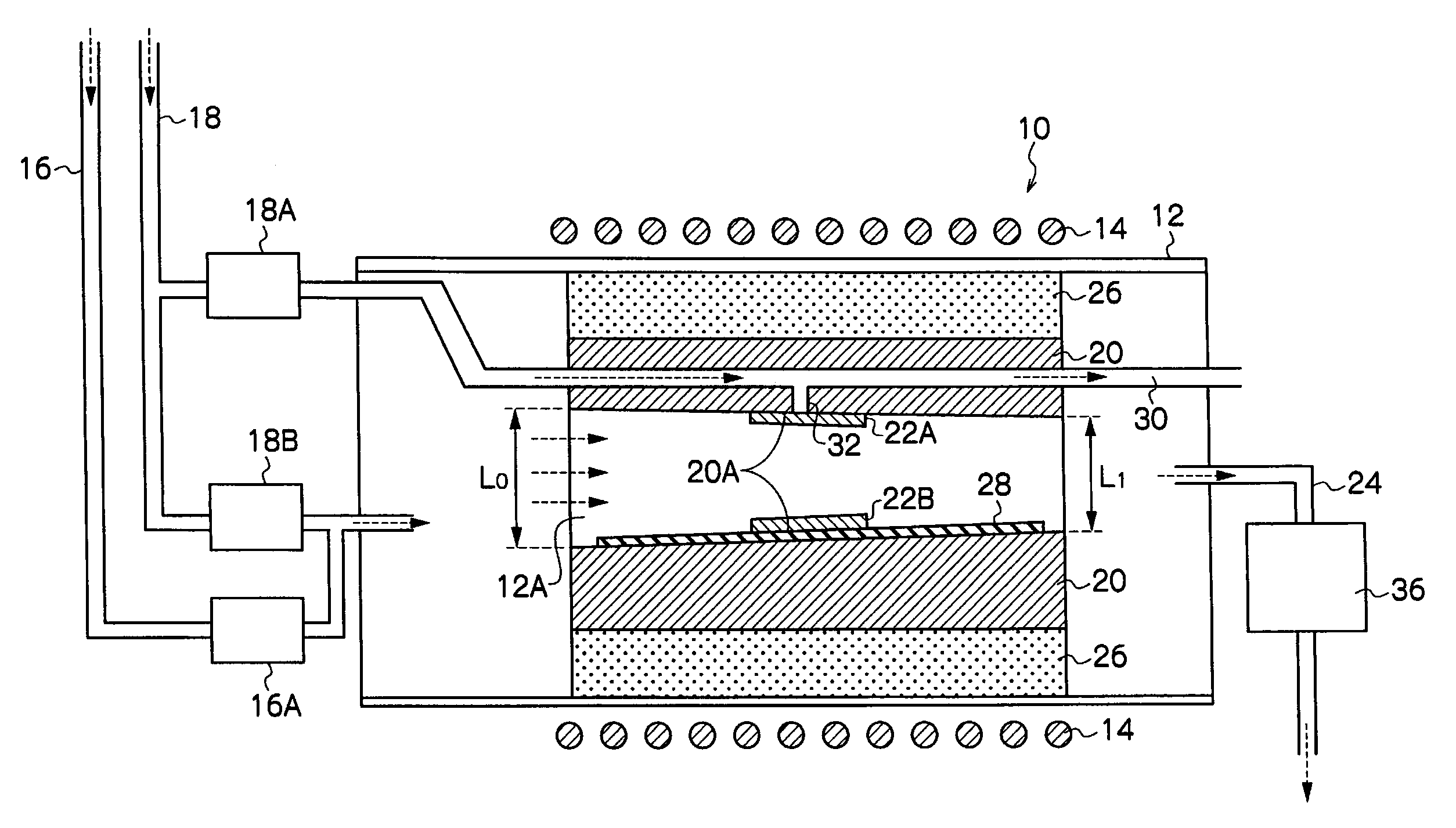
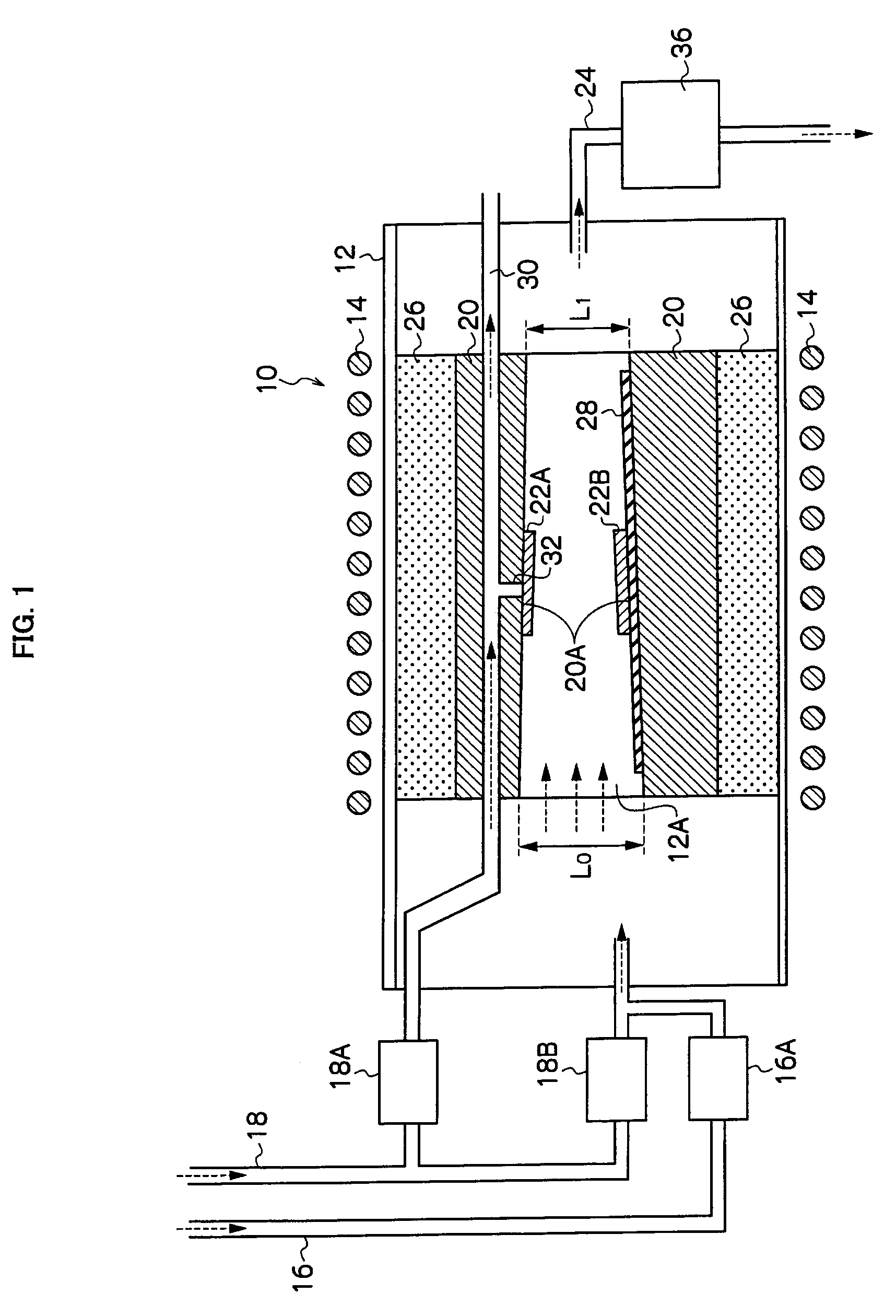
[0054]Formation of an SiC epitaxial thin film on a substrate was conducted using a semiconductor thin film manufacturing apparatus shown in FIG. 1. The substrate was held by distributing a carrier gas (hydrogen gas: 100 sccm) in a through hole 30 (diameter: 8 mm) while temporarily holding the substrate by a holding member 50, as shown in FIG. 4 illustrating a cross-sectional view of the reaction tube 12. The diameter of a communicating part was 8 mm.

[0055]The substrate used was a 4H-SiC wafer with a 8° off (0001) Si face. Epitaxial growth was performed by chemical vapor deposition (CVD method). The apparatus used was a horizontal hot wall-type CVD apparatus. Other growth conditions and results are shown in the following Table 1. As seen from Table 1, falling of foreign matters onto the substrate placed on the upper side and deposition of a thin film to the back surface of the substrate were not observed, and in-plane evenness was favorable. The number of defects and the presence or ...

example 2

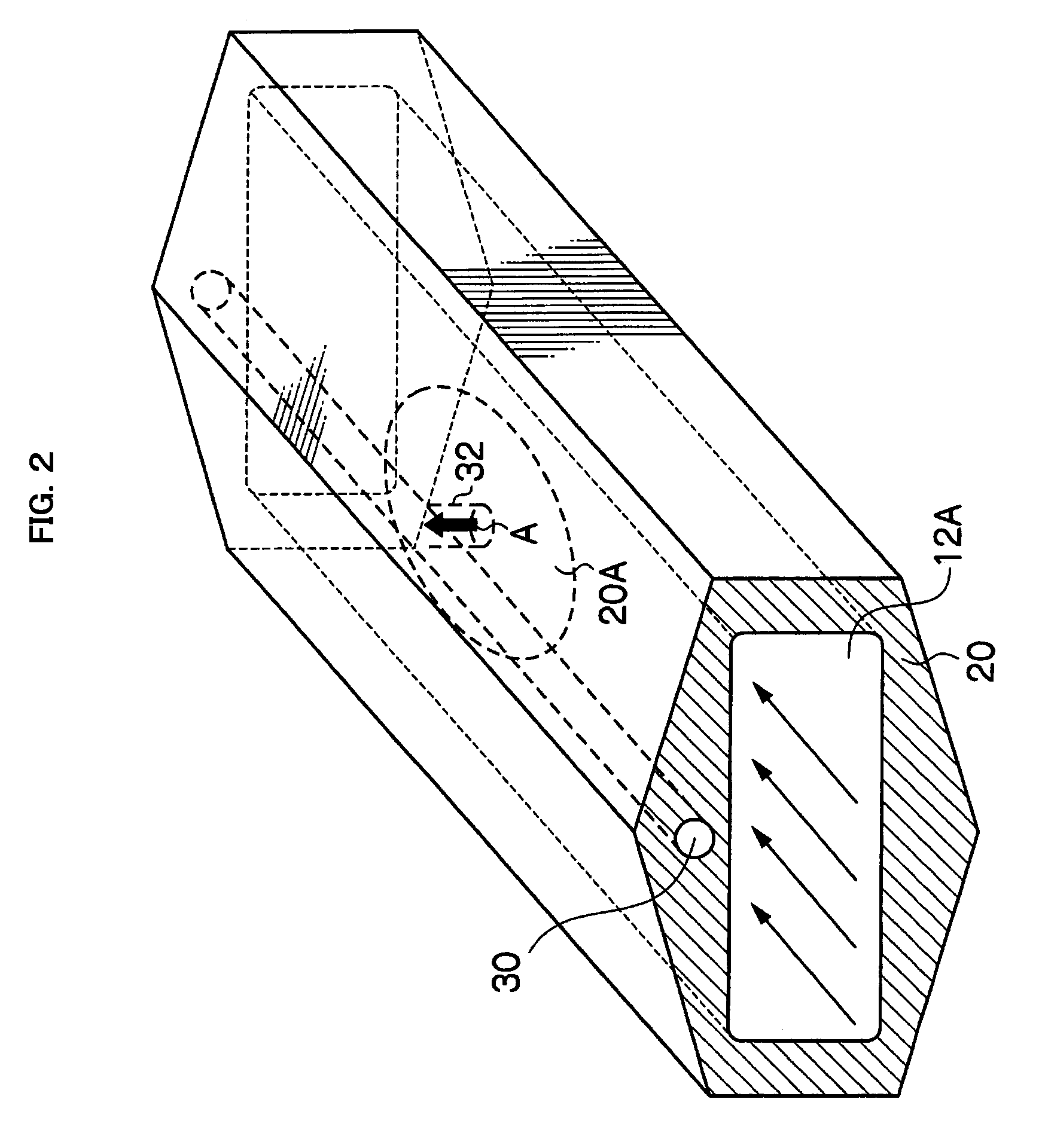
[0056]Formation of an SiC epitaxial thin film on a substrate was conducted using a semiconductor thin film manufacturing apparatus equipped with a similar susceptor to that used in Example 1, except that a through hole had a venturi structure as shown in FIG. 3. Angles θ1, θ2, θ3 and θ4 were 8°, respectively. The diameters of both ends of the through hole were 8 mm, respectively. Other growth conditions and results are shown in the following Table 1. As seen from Table 1, falling of foreign matters onto the substrate placed on the upper side and deposition of a thin film to the back surface of the substrate were not observed, and in-plane evenness was favorable.


PUM

PropertyMeasurementUnit
Angleaaaaaaaaaa
Angleaaaaaaaaaa
Angleaaaaaaaaaa

Abstract

The present invention provides an apparatus for manufacturing a semiconductor thin film that is capable of manufacturing an even thin film with substantially no adhesion of impurities, and is capable of improving in-plane evenness of a grown thin film. The invention is an apparatus for manufacturing a semiconductor thin film includes a reaction tube 12, a susceptor 20 disposed in the reaction tube 12, and a negative pressure generator, the negative pressure generator applying a negative pressure to a substrate 22A placed on the susceptor 20 to hold the substrate, and the substrate 22A is placed so that an angle of a normal line to a crystal growth face of the substrate 22A to a vertical downward direction is less than 180°.

Description

TECHNICAL FIELD[0001]The present invention relates to an apparatus for manufacturing a semiconductor thin film that manufactures a silicon carbide semiconductor, more particularly a semiconductor thin film manufacturing apparatus that forms a semiconductor thin film on a substrate by epitaxial growth.BACKGROUND ART[0002]Silicon carbide (SiC) semiconductors, for example, having excellent heat resistance and mechanical strength, have been attracting attention for such reasons as their use as a material in blue light-emitting diodes and the like, and their application to electric elements having high power and low loss due to the demand for energy saving through high pressure resistance and low ion resistivity. An SiC semiconductor is formed by depositing an SiC thin film on an SiC substrate. As a means of depositing an SiC thin film on a substrate to form an SiC semiconductor, for example, epitaxial growth of SiC can be utilized.[0003]The SiC thin film is deposited on the substrate by...

Claims


Application Information

Patent Timeline
IPC IPC(8): C23C16/00
CPCC23C16/325C23C16/4583H01L21/02529C30B29/36H01L21/02378C30B25/12
Inventor SAITOH, HIROAKI
Owner TOYOTA JIDOSHA KK
Why Eureka
Try Eureka