Integrated circuits for testing an active matrix display array

a technology of integrated circuits and active matrix, which is applied in the direction of electronic circuit testing, measurement devices, instruments, etc., can solve the problems of cost-effective solutions and high cost of design modifications

Inactive Publication Date: 2005-09-06
VIDEOCON GLOBAL
View PDF22 Cites 21 Cited by
  • Summary
  • Abstract
  • Description
  • Claims
  • Application Information

AI Technical Summary

Benefits of technology

[0010]The problems stated above and the related problems of the prior art are solved with the principles of the present invention, integrated circuits for display arrays. The present invention provides a device for use in a display system comprising an array of pixel cells formed on a substrate. Each pixel cell is coupled to at least one gate line of a plurality of gate lines formed on the substrate and at least one data line of a plurality of data lines formed on the substrate. The device comprises first and second transistors formed on said substrate. Each transistor has a gate electrode and first and second electrodes defining a serpentine channel region there between. Voltage applied to the gate electrode controls conductivity of the channel region. Preferably, the a common electrode comprises one of the first and second electrodes of said first transistor and one of said first and second electrodes of said second transistor. The first and second transistors are preferably coupled between a gate line (or data line) and respective probe pads formed on the substrate and selectively couple the respective probe pad to the gate line (or data line) during a test routine whereby charge is written to, stored, and read from the array of pixel cells.

Problems solved by technology

In order to test such an array, the probe fixture for the gate lines and / or data lines must be redesigned to accommodate for the variation in spacing, which is a costly solution.
Such design modifications are also very costly.

Method used


Image

  • Integrated circuits for testing an active matrix display array
  • Integrated circuits for testing an active matrix display array
  • Integrated circuits for testing an active matrix display array

Examples


Embodiment Construction

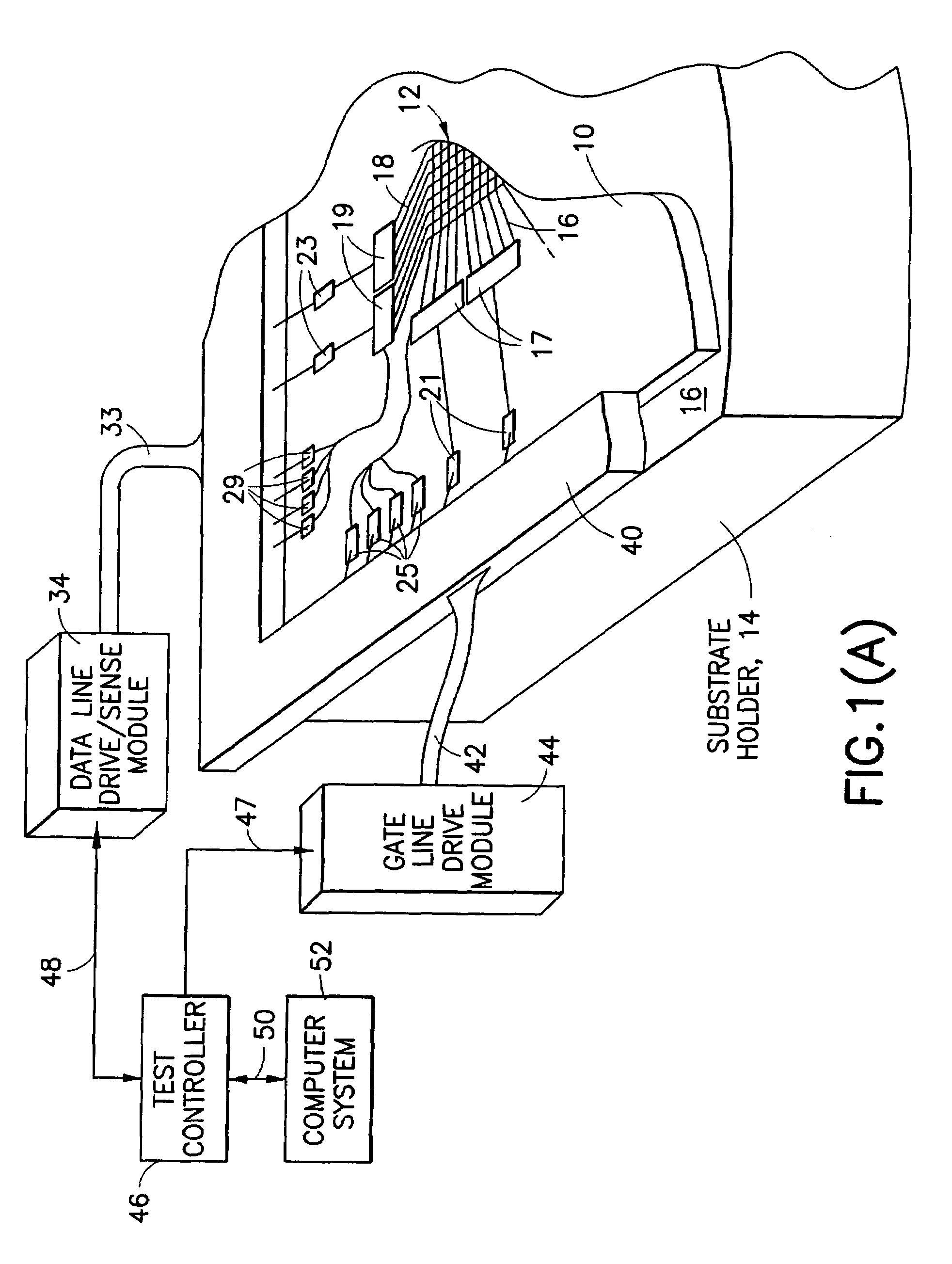
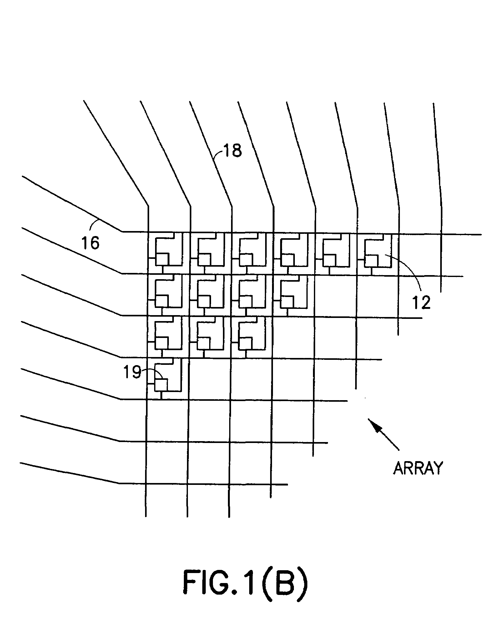
[0026]Referring to FIG. 1(A), a substrate 10 having formed thereon an array of TFT / LC pixel cells 12 is supported on a substrate holder 14. Substrate 10 has a number of gate lines 16 and data lines 18 formed thereon that are electrically coupled to the TFTs (not shown) of the cells to drive the array of cells 12. FIG. 1(B) illustrates the array of cells 12 formed on the substrate 10. Each pixel cell 12 includes a TFT 19 coupled to a gate line 16 and data line 18.

[0027]The basic routine for testing the array is as follows: biasing the gate line 16 and data line 18 connected to a cell 12 such that the TFT of the cell 12 is in a conductive (ON) state and charge is written to the cell 12, storing the charge in the cell 12 by biasing the gate line 16 and data line 18 connected to the cell 12 such that the TFT of the cell 12 is in a nonconductive (OFF) state, and reading the charge stored in the cell 12. Reading the charge stored in a cell 12 is accomplished by electrically coupling sense...


PUM


Abstract

A device for use in a display system including an array of pixel cells formed on a substrate. Each pixel cell being coupled to at least one gate line of a plurality of gate lines formed on the substrate and at least one data line of a plurality of data lines being formed on the substrate. The device includes first and second transistors formed on the substrate. Each transistor has a gate electrode and first and second electrodes defining a serpentine channel region there between voltage applied to the gate electrode controls conductivity of the channel region. Preferably, a common electrode includes one of the first and second electrodes of the first transistor and one of the first and second electrodes of the second transistor. The first and second transistors are preferably coupled between a gate line (or data line) and respective probe pads formed on the substrate and selectively couple the respective probe pad to the gate line (or data line) during a test routine whereby charge is written to, stored, and read from the array of pixel cells.

Description

PRIORITY[0001]This application claims priority to now abandoned Provisional application filed Sep. 23, 1998, assigned Ser. No. 60 / 100,889, having the same title, which is included herein by reference in entirety for all purposes.BACKGROUND OF THE INVENTION[0002]1. Technical Field[0003]The invention relates to liquid crystal display (LCD) arrays.[0004]2. Description of the Related Art[0005]An array tester as described in U.S. Pat. No. 5,179,345 and 5,546,013 provides a means for testing the cells of an TFT / LCD display array by coupling test probes to the gate line pads and data line pads that terminate the gate lines and data lines, respectively, of the TFT / LCD array.[0006]Importantly, when the size of the TFT / LCD display array under test is changed, the spacing of the gate lines and / or data lines and the pads terminating thereof change. In order to test such an array, the probe fixture for the gate lines and / or data lines must be redesigned to accommodate for the variation in spacin...

Claims


Application Information

Patent Timeline
Patent Type & Authority Patents(United States)
IPC IPC(8): G01R31/00G09G3/00G09G3/36
CPCG09G3/006G09G3/3648
Inventor JENKINS, LESLIE CHARLESLIBSCH, FRANK ROBERTMASTRO, MICHAEL PATRICKNYWENING, ROBERT WAYNEPOLASTRE, ROBERT JOHN
Owner VIDEOCON GLOBAL
Why Eureka
Try Eureka