Smart card or similar electronic device

a technology of electronic devices and smart cards, applied in the field of smart cards or similar electronic devices, can solve the problems of production rejection, difficult operation, limited association cost, etc., and achieve the effect of reducing the cost and the percentage of production rejection

Inactive Publication Date: 2005-09-13
GEMPLU
View PDF5 Cites 35 Cited by
  • Summary
  • Abstract
  • Description
  • Claims
  • Application Information

AI Technical Summary

Benefits of technology

[0019]The basic purpose of the invention is to provide a method for making connections between a microcircuit and the interface elements in an electronic unit (such as a smart card) including at least one microcircuit which is embedded in a carrier medium and which includes exit hubs linked to interface elements including a terminal block and / or an antenna which do not have the above-mentioned disadvantages and which make it possible in particular to reduce the cost and percentage of production rejects without making micromodules.
[0021]This method makes it possible to eliminate the making of micromodules and to reduce the number of production steps.
[0022]In addition, flexible connections are obtained whereas the connections of the known type are rigid or semi-rigid, and this sharply reduces the rate of production rejects.
[0023]Advantageously, the terminal block is also made by depositing a low-viscosity conducting substance. This makes it possible to further simplify the method with the making of the terminal block and its connections in a single operation.
[0024]Advantageously, the antenna is also made by depositing a low-viscosity conducting substance. This makes it possible to simplify the production and to improve the antenna performance.

Problems solved by technology

In the methods which use a micromodule, the associated costs are limited by the price of the film.
This operation is difficult because the resin is polymerized and thus very rigid.
The milling is the main cause of production rejects.
In the first method without micromodules described above, this resin is on the surface and thus subject to exterior stresses, greatly increasing the associated cost.
For the second method without micromodules the number of steps is high, which also increases the cost.
This technology would therefore not be suitable for making large chip cards.
Such a technique can only be used for chips with simple operation.
In these methods for making smart cards without contacts, micromodule manufacturing is used which, as mentioned above, involves numerous steps for assembling the chip and implies substantial costs, or the “flipchip” technique for which the pace is limited and the installation costs particularly high.
The methods for hybrid smart cards combine the disadvantages previously mentioned for smart cards both with and without contacts.
In addition, flexible connections are obtained whereas the connections of the known type are rigid or semi-rigid, and this sharply reduces the rate of production rejects.

Method used


Image

  • Smart card or similar electronic device
  • Smart card or similar electronic device
  • Smart card or similar electronic device

Examples


Embodiment Construction

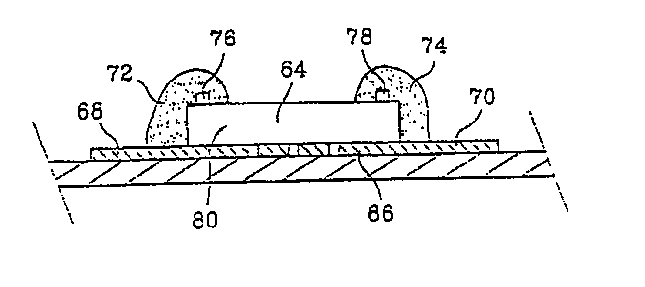
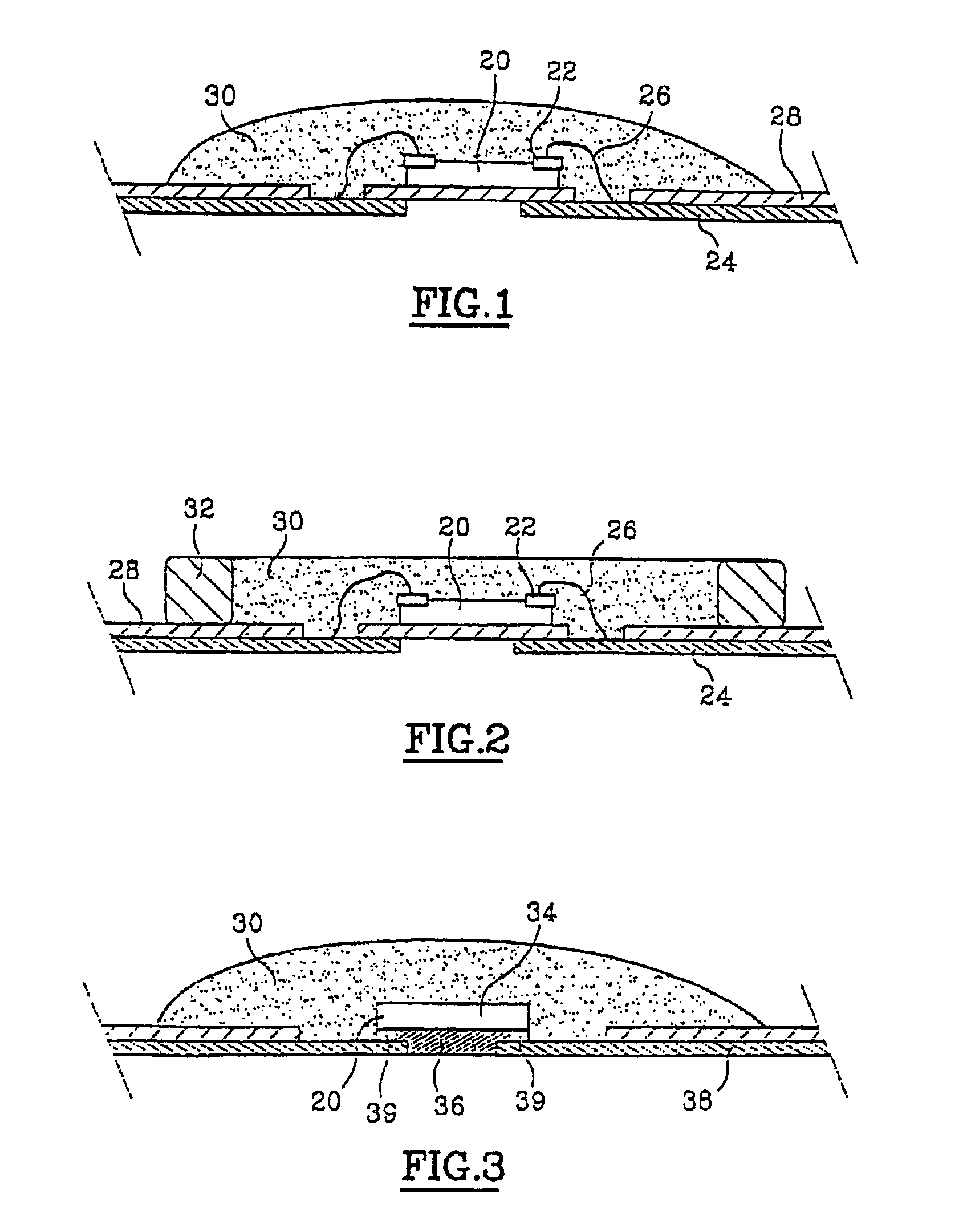
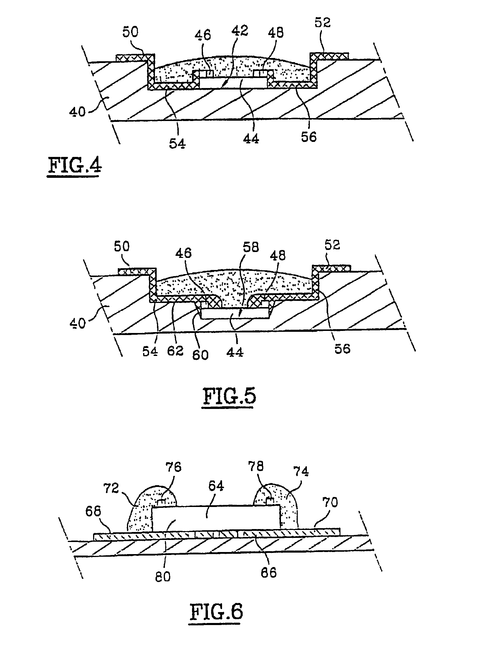
[0036]FIG. 4 shows a smart card with contacts made according to a method of the present invention. Initially, a card body 40 is made which includes a cavity 42 which can be made by injection molding or by colamination of thermoplastic sheets followed by machining of the cavity.

[0037]In a second step, the chip 44 is placed in the cavity with its active side, and particularly its exit hubs 46 and 48, facing upwards, and it is attached by gluing, for example. Local heating of the cavity can also be done followed by placing the chip in the molten thermoplastic material. The active side of the chip does not have to be on the same level as the bottom of the cavity.

[0038]In a third step, the contact terminal block and the connections with the exit hubs 46 and 48 are made by depositing a low-viscosity conducting substance, for example a polymer resin charged with conducting or intrinsically conducting particles, by a technique called “dispensing” by which a liquid or low-viscosity substance...


PUM


Abstract

The invention concerns an electronic device such as a smart card which includes at least a microcircuit embedded in a carrier medium and which includes exit hubs linked to interface elements composed of a terminal block and / or an antenna. The connections between the exit hubs and the interface elements are made by depositing a low-viscosity conducting substance which remains flexible after its application, using a syringe or similar device. Preferably, a polymer resin charged with conducting or intrinsically conducting particles is used for the connections.

Description

[0001]This disclosure a continuation of U.S. application Ser. No. 09 / 381,797, filed Sep. 24, 1999 now U.S. Pat. No. 6,468,835 which was based upon, and claimed priority from, French Patent Application No. 97 / 04093, filed Mar. 27, 1997, and which was a national stage filing under 35 U.S.C. § 371 of International Application No. PCT / FR98 / 00592, filed Mar. 25, 1998, the contents of each of which are incorporated herein by reference.FIELD OF THE INVENTION[0002]The present invention concerns the making of electronic units including at least one microcircuit which is embedded in a carrier medium and linked to interface elements consisting of a terminal block and / or an antenna, such as integrated circuit cards with or without contacts, also known as smart cards. The invention also applies, in particular, to electronic labels which are used to identify products and which can be compared with smart cards without contacts. The present invention concerns more particularly the making of connect...

Claims


Application Information

Patent Timeline
IPC IPC(8): G06K19/077G06K19/07B42D15/10
CPCG06K19/07743G06K19/07749G06K19/0775G06K19/07769G06K19/07779G06K19/07783H01L24/24H01L24/82H01L2924/07802H01L2224/48227H01L2224/16225H01L2224/24051H01L2224/24225H01L2224/24226H01L2224/24227H01L2224/48091H01L2224/48228H01L2924/01015H01L2924/01033H01L2924/01057H01L2924/01058H01L2924/01059H01L2924/01074H01L2924/01078H01L2924/01079H01L2924/01082H01L2924/14H01L2924/15153H01L2924/15165H01L2924/19042H01L2924/01006H01L2924/01087H01L2924/014H01L2224/16227H01L2924/00014H01L2924/00G06K19/077
Inventor BLANC, RENE-PAULFIDALGO, JEAN-CHRISTOPHEPATRICE, PHILIPPE
Owner GEMPLU
Why Eureka
Try Eureka