Suppression of MOSFET gate leakage current

a technology of leakage current and mosfet, which is applied in the field of mosfet fabrication, can solve the problems of extremely difficult or impossible energetically available and/or accessible charge-carrier tunneling states, and achieve the effect of significant reducing gate leakage curren

Inactive Publication Date: 2005-09-27
TAIWAN SEMICON MFG CO LTD
View PDF20 Cites 69 Cited by
  • Summary
  • Abstract
  • Description
  • Claims
  • Application Information

AI Technical Summary

Benefits of technology

[0005]The primary object of this invention is to provide a method for significantly reducing gate leakage currents under a variety of operating conditions within a MOSFET having a thin gate dielectric.
[0010]4. When the full supply voltage VDD is applied to the drain and the gate is at zero bias, both the gate and drain regions in the gate / drain overlap region will be depleted of charge carriers. In this condition the lack of free carriers in the vicinity of the gate dielectric will significantly reduce or eliminate leakage current between the gate and drain in the overlap region.

Problems solved by technology

The method involves gate-material engineering, selecting a particular gate electrode material, channel material and dielectric material such that there can be obtained an alignment of their band structures that makes the availability and / or the accessibility of charge-carrier tunneling states energetically extremely difficult or impossible.

Method used


Image

  • Suppression of MOSFET gate leakage current
  • Suppression of MOSFET gate leakage current
  • Suppression of MOSFET gate leakage current

Examples


Embodiment Construction

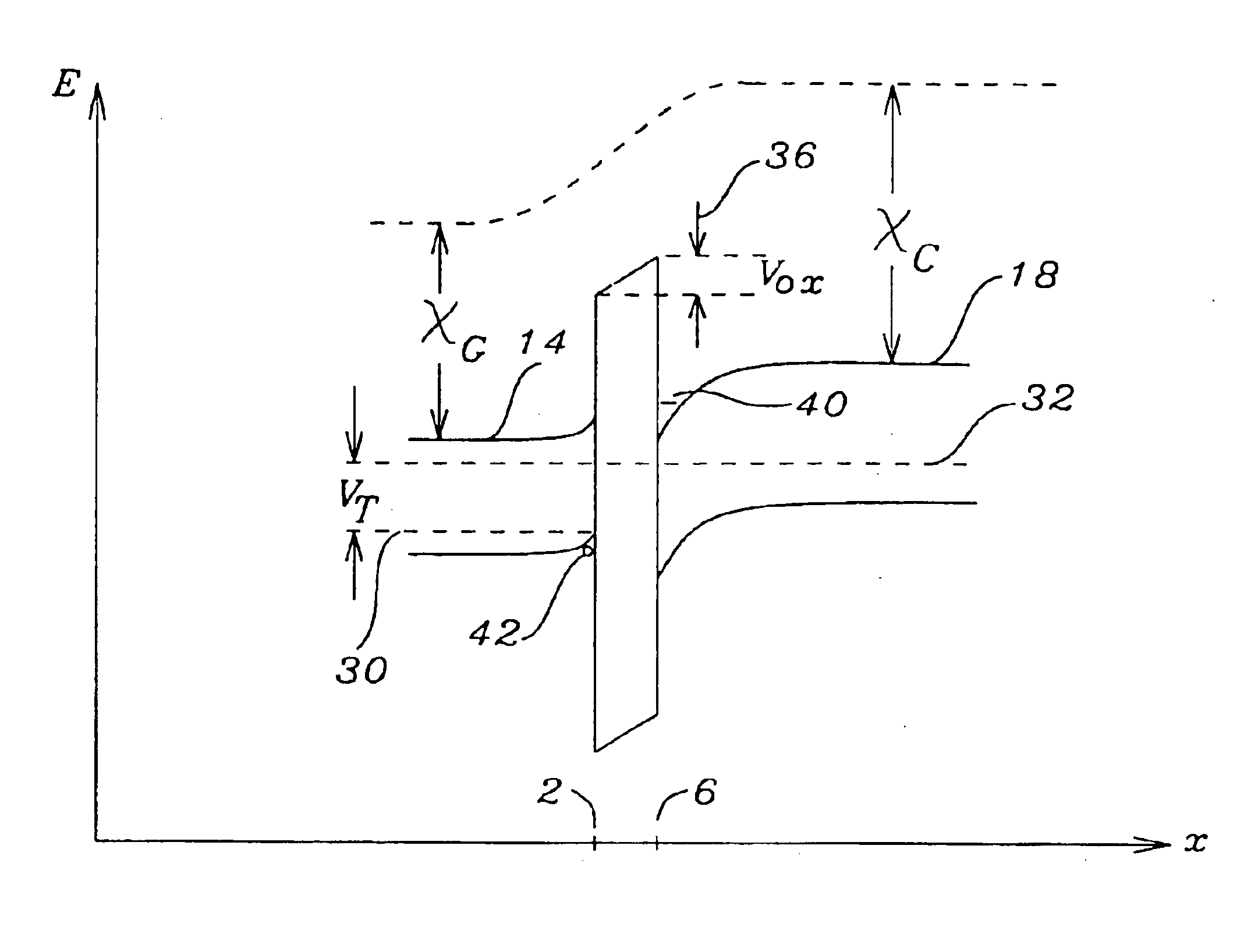
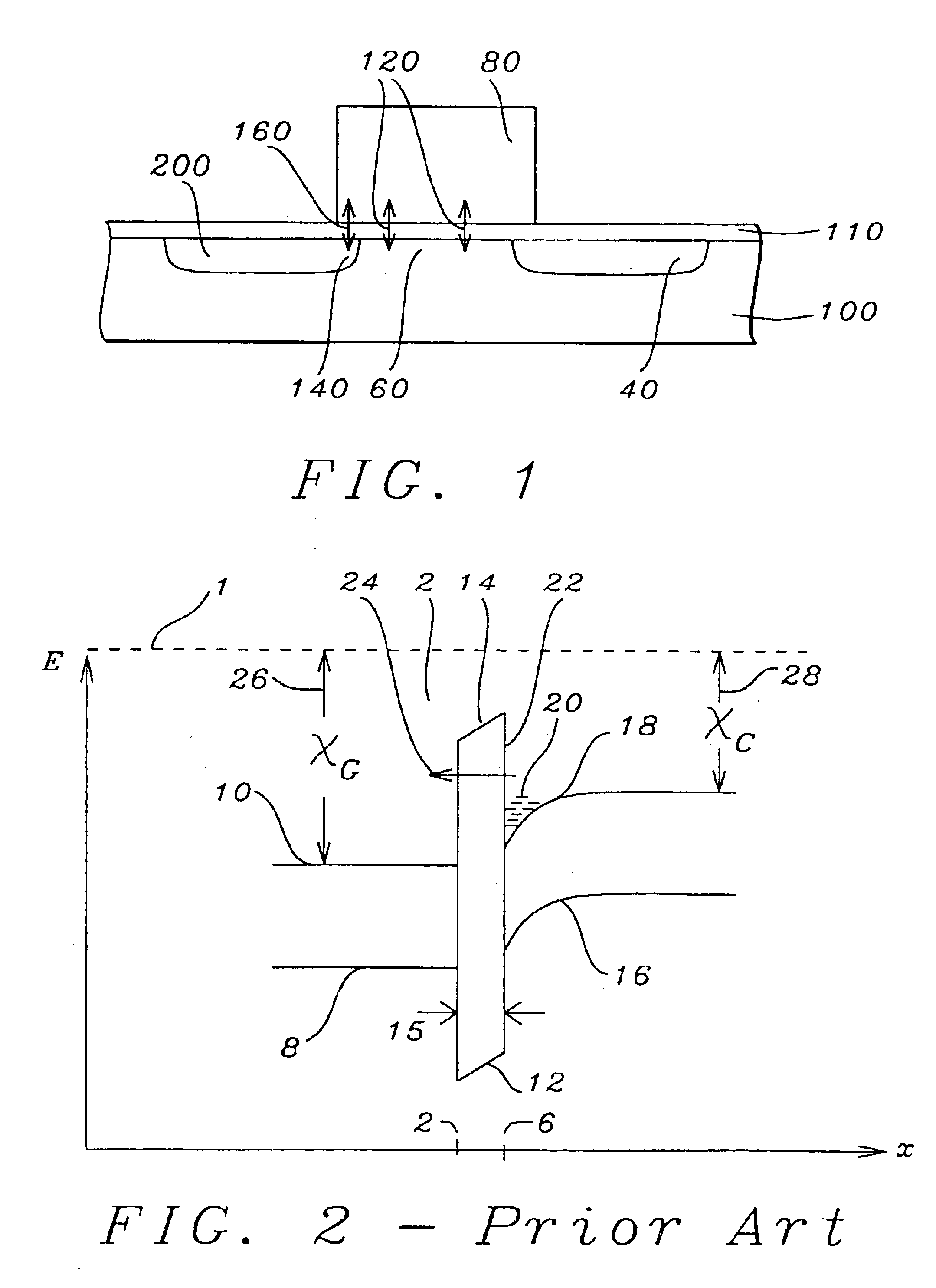
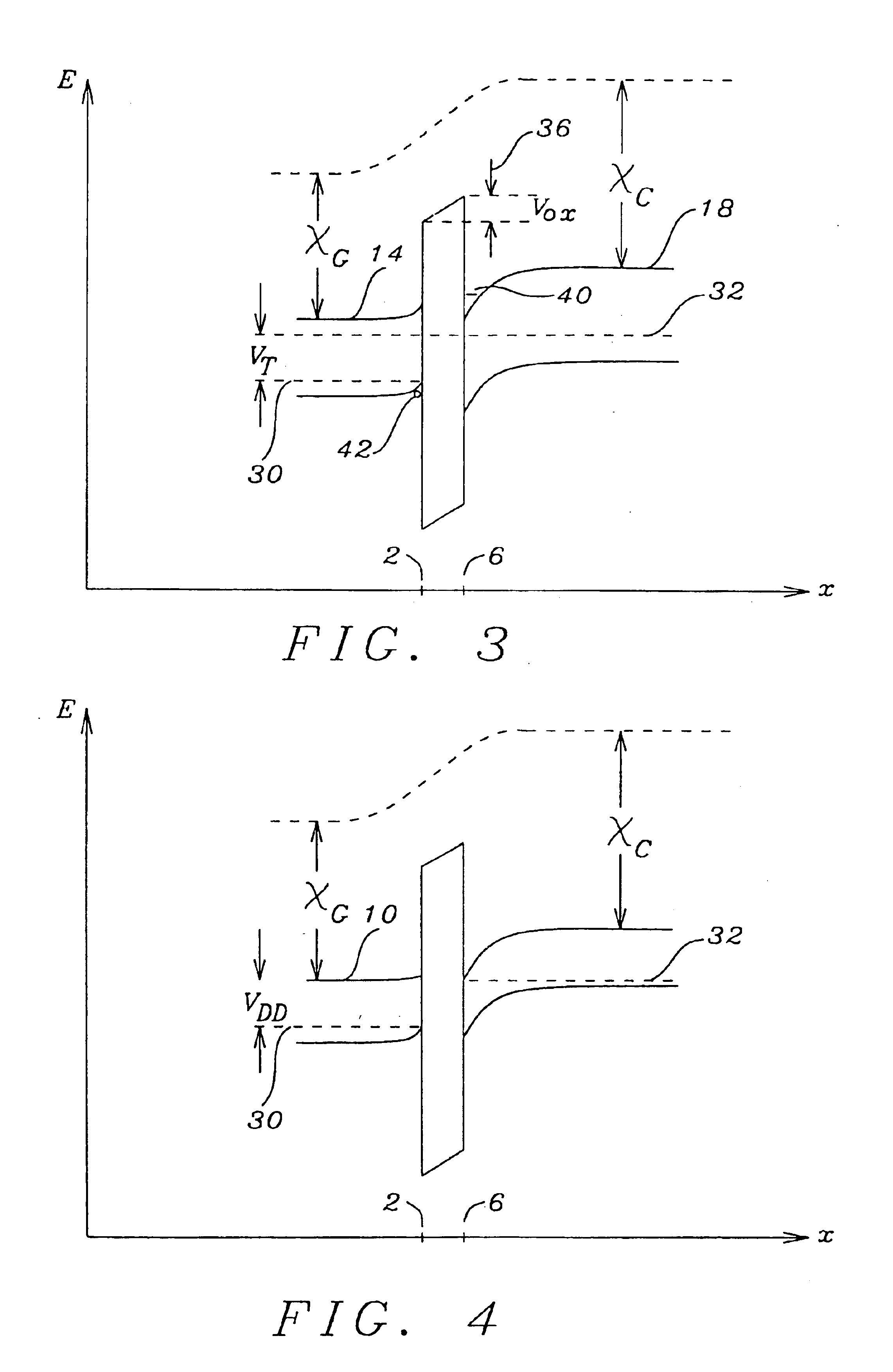
[0018]The preferred embodiment of the present invention provides a method of significantly reducing undesirable leakage currents between the gate electrode of a MOSFET and its channel, source or drain regions. It is understood that the MOSFET has a very thin dielectric layer between the gate and body of the substrate, so the mechanism for leakage currents is primarily carrier tunneling between the gate and the other regions of the transistor, across the dielectric layer. It is further understood that such tunneling can occur only when there are available states for the charge carrier to tunnel to. The lack of available states in the region to which the carrier is tunneling will produce a zero probability of tunneling. It is the object of this invention to effectively eliminate these available states by properly matching the energy band diagrams of the gate electrode material and the material of the channel region (or source region). In the following description, the preferred embodi...


PUM


Abstract

A MOSFET has greatly reduced leakage current between the gate electrode and the channel, source and drain regions. The gate electrode materials have lower electron affinities than the channel, source and drain regions. Gate electrode materials with negative electron affinities can also be used. The use of these gate electrode materials enables the band structures of the gate electrode and the other regions to be aligned in a manner that eliminates tunneling states for carriers tunneling between the gate and the body of the device.

Description

RELATED APPLICATION[0001]This application is a divisional of U.S. patent application Ser. No. 10 / 245,428 filed Sep. 17, 2002 now U.S. Pat. No. 6,830,953, and entitled, “Suppression of MOSFET Gate Leakage Current,” which is hereby incorporated by reference in its entirety.BACKGROUND OF THE INVENTION[0002]This invention relates generally to the fabrication of MOSFETs, and more particularly to the selection and method of use of novel materials to suppress gate leakage currents in these devices under various operating conditions as their dimensions are reduced.[0003]As the dimensions of MOSFETS (Metal Oxide Semiconductor Field-Effect Transistors) continue to shrink, the reduced length of the channel between source and drain causes unwanted side-effects (short-channel effects) due to the increased electric field intensity therein. One way in which such effects have been addressed is by forming an asymmetric lightly doped drain within the transistor, a method taught by Chien et al. (U.S. ...

Claims


Application Information

Patent Timeline
Patent Type & Authority Patents(United States)
IPC IPC(8): H01L29/40H01L29/66H01L29/78H01L29/49
CPCH01L29/78H01L29/49
Inventor HU, CHENMINGYEO, YEE-CHIA
Owner TAIWAN SEMICON MFG CO LTD
Why Eureka
Try Eureka