Liquid crystal display device having a higher contrast ratio

a liquid crystal display and contrast ratio technology, applied in non-linear optics, instruments, optics, etc., can solve the problems of degrading the contrast ratio, reducing the intensity of scattered light caused by one of the interconnect lines extending in the pixel area, and not effectively preventing light from being scattered by the side surfaces of the interconnect lines.

Inactive Publication Date: 2005-09-27
NEC LCD TECH CORP
View PDF3 Cites 13 Cited by
  • Summary
  • Abstract
  • Description
  • Claims
  • Application Information

AI Technical Summary

Benefits of technology

[0009]In view of the above problem in the conventional LCD device, it is an object of the present invention to provide a LCD device capable of suppressing the scattering of light within the LCD panel and thus achieving a higher contrast ratio.
[0011]In accordance with the LCD device of the present invention, the intensity of scattered light caused by the one of the interconnect lines extending in the pixel area can be reduced due to the lower surface reflectance of the one of the interconnect lines, whereas the another of the interconnect lines extending outside the pixel area has a lower line resistance to achieve a desired operational speed.

Problems solved by technology

If aluminum interconnect lines having a higher surface reflectance are provided in the pixel area through which light passes, especially in the IPS LCD device, it is likely to cause scattering of light.
Accordingly, the restriction of the amount of light components obliquely passing in the LCD panel, as described in the publication, does not effectively prevent the light from being scattered by the side surfaces of the interconnect lines.
Thus, a higher black brightness is caused to degrade the contrast ratio, whereby the improvement in the contrast ratio is not sufficient in the LCD devices.

Method used


Image

  • Liquid crystal display device having a higher contrast ratio
  • Liquid crystal display device having a higher contrast ratio
  • Liquid crystal display device having a higher contrast ratio

Examples


Embodiment Construction

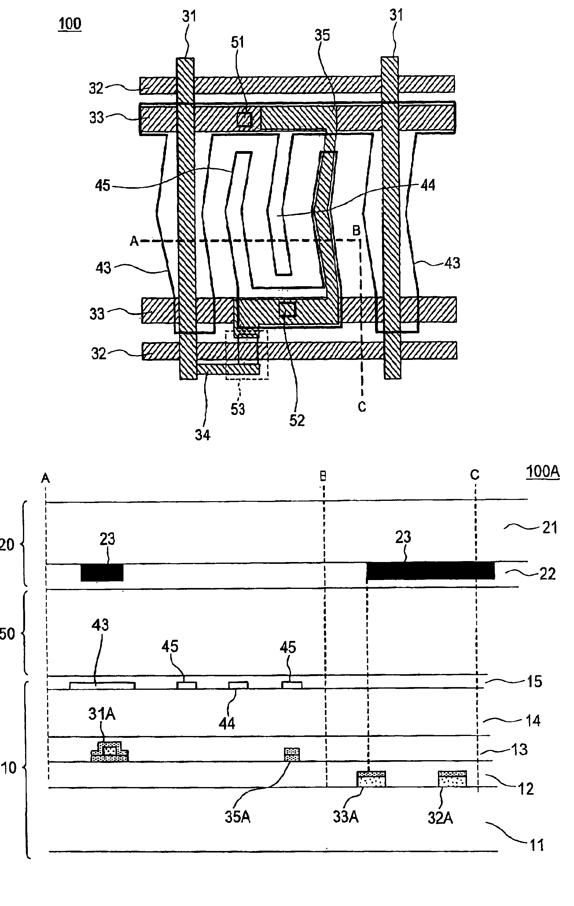
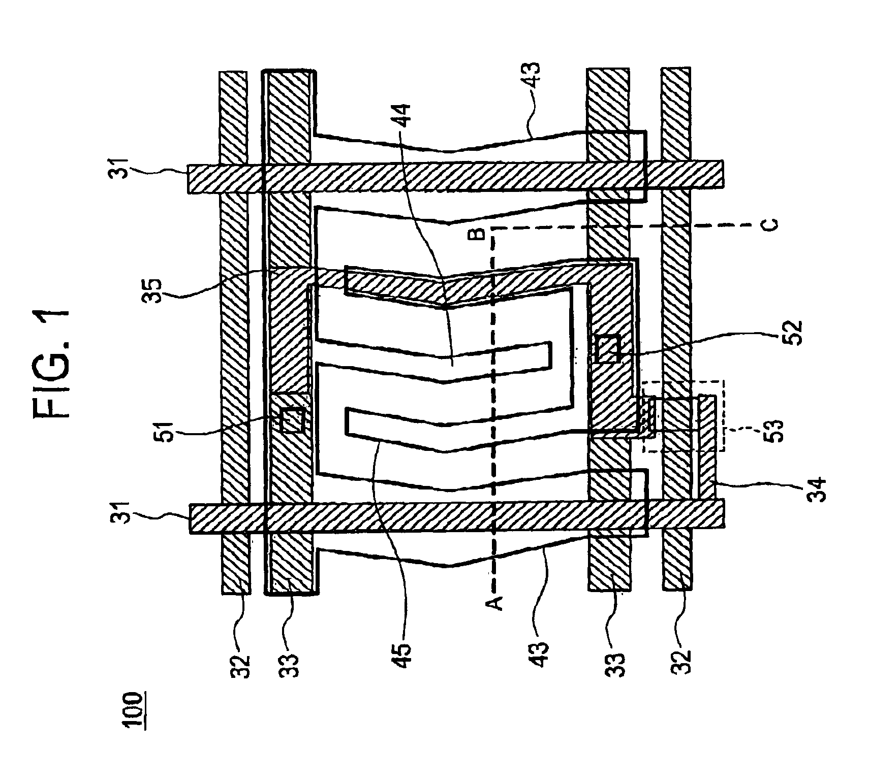
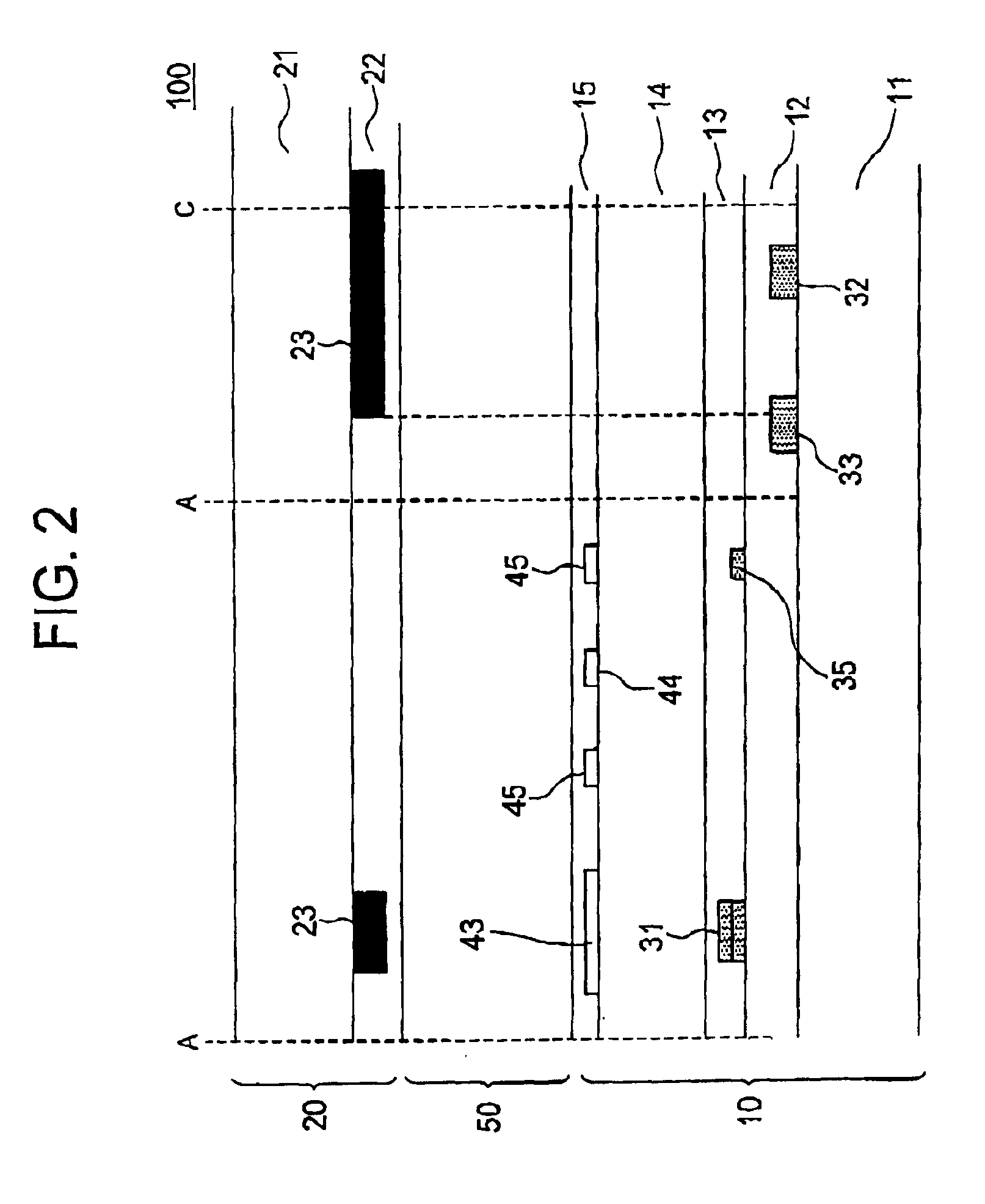
[0018]Now, the present invention is more specifically described with reference to accompanying drawings, wherein similar constituent elements are designated by similar reference numerals throughout the drawings.

[0019]Referring to FIG. 1, a LCD device, generally designated by numeral 100, according to a first embodiment of the present invention is implemented as an IPS LCD device, wherein the LC layer sandwiched between a pair of LCD panels is applied with a lateral electric field. The LCD device 100 includes a plurality of pixels arranged in an array, a plurality of signal lines 31 extending in the column direction of the array, a plurality of scanning lines 32 extending in the row direction of the array, and a plurality of common electrode lines 33 extending parallel to the scanning lines 32.

[0020]Each pixel has a pixel area defined by adjacent two of the signal lines 31 and adjacent two of the scanning lines 32. Each pixel includes a drain electrode line 34 extending from a corres...


PUM

PropertyMeasurementUnit
viewing angleaaaaaaaaaa
oblique anglesaaaaaaaaaa
areaaaaaaaaaaa

Abstract

A LCD device has a black matrix defining a plurality of pixel areas in the LCD device. An interconnect layer formed on a TFT panel includes a first interconnect line passing through the pixel area and a second interconnect line passing outside the pixel area. The first interconnect line is lower in a product of a thickness thereof by a surface reflectance thereof than the second interconnect line.

Description

BACKGROUND OF THE INVENTION[0001](a) Field of the Invention[0002]The present invention relates to liquid crystal display (LCD) device having a higher contrast ratio and, more particularly, to a LCD device including an interconnect line having a lower surface reflectance.[0003](b) Description of the Related Art[0004]LCD devices are used in a variety of fields such as household use or medical use, and the number of fields in which the LCD devices are used are increasing. In general, the LCD device includes a pair of polarization plates disposed at the backlight side and the front side of a LCD panel and sandwiching therebetween the LCD panel. The polarization plates have respective polarization axes perpendicular to each other. By applying an electric field to the liquid crystal (LC) layer in the LCD device, the light components passing through the LC layer and polarization plate disposed at the front side are controlled for display of a desired image.[0005]In the LCD device, the term...

Claims


Application Information

Patent Timeline
Patent Type & Authority Patents(United States)
IPC IPC(8): G02F1/13G02F1/1343G02F1/1335
CPCG02F1/134363G02F1/133512
Inventor KADOTANI, TSUTOMU
Owner NEC LCD TECH CORP
Why Eureka
Try Eureka