Packaged microelectronic component assemblies

a technology of microelectronic components and components, applied in the direction of electrical equipment, semiconductor devices, semiconductor/solid-state device details, etc., can solve the problem that both options may prove unduly expensiv

Active Publication Date: 2005-10-04
MICRON TECH INC
View PDF149 Cites 159 Cited by
  • Summary
  • Abstract
  • Description
  • Claims
  • Application Information

AI Technical Summary

Problems solved by technology

For highly cost-competitive products, such as memory mo

Method used


Image

  • Packaged microelectronic component assemblies
  • Packaged microelectronic component assemblies
  • Packaged microelectronic component assemblies

Examples


Embodiment Construction

A. Overview

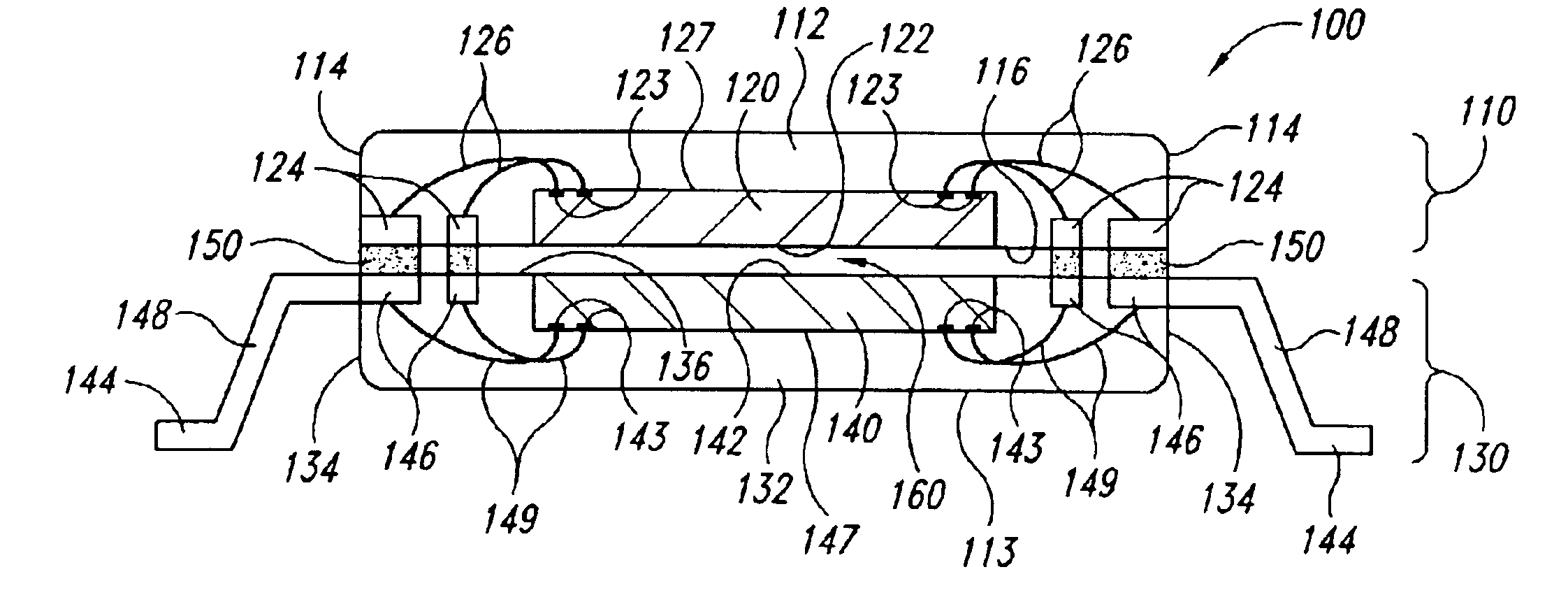
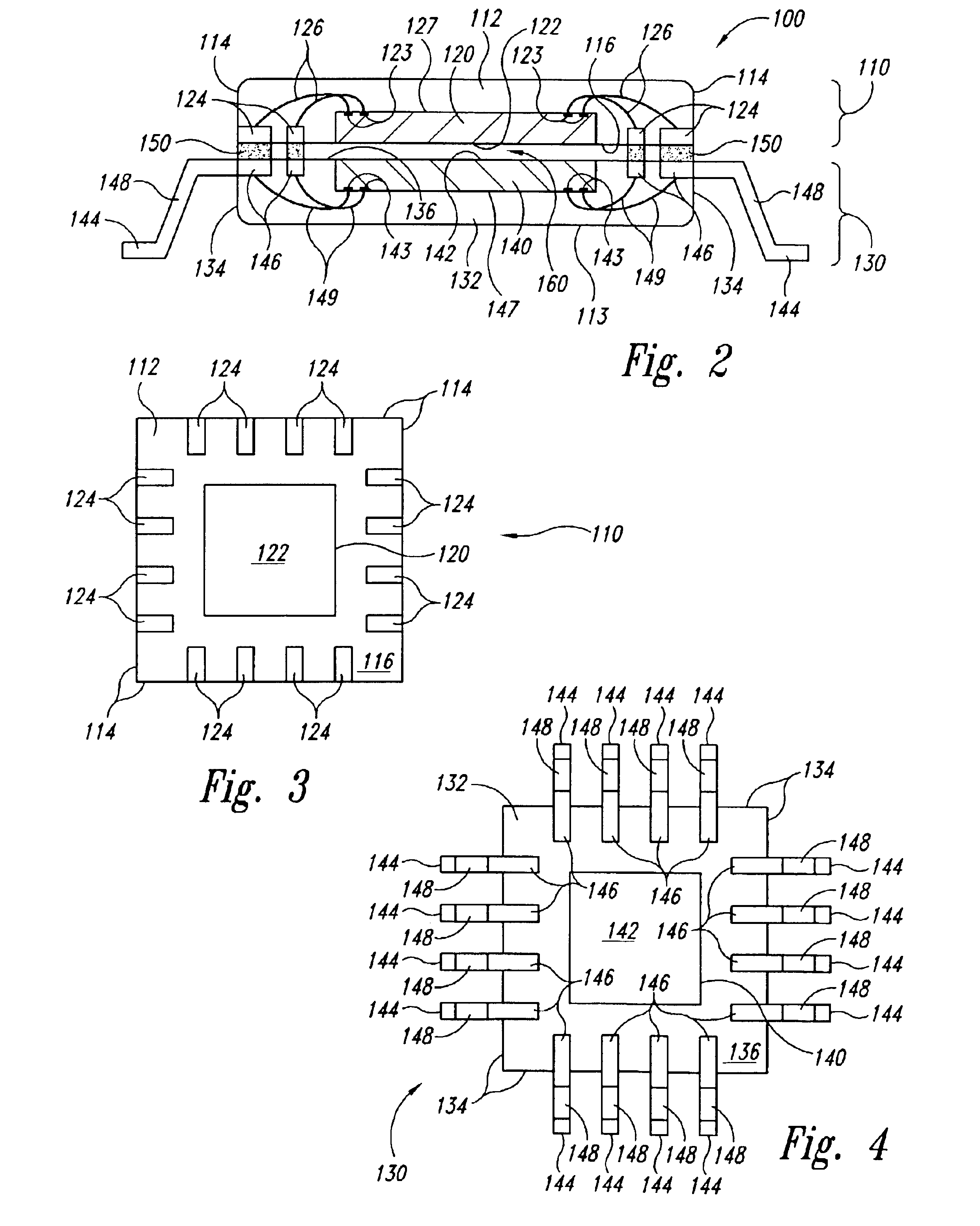
[0022]Various embodiments of the present invention provide microelectronic component assemblies, memory modules, computer systems, and methods for forming microelectronic component assemblies, memory modules, and computer systems. The terms “microelectronic component” and “microelectronic component assembly” may encompass a variety of articles of manufacture, including, e.g., SIMM, DRAM, flash-memory, ASICs, processors, flip chips, ball grid array (BGA) chips, or any of a variety of other types of microelectronic devices or components therefor.

[0023]One embodiment provides a microelectronic component assembly that includes first and second microelectronic component packages. The first package includes a first microelectronic component having a back surface and a first mold compound formed about the first microelectronic component, with the first mold compound also having a back surface. The first package also includes a plurality of first package contacts and a plurality ...


PUM

PropertyMeasurementUnit
Lengthaaaaaaaaaa
Flow rateaaaaaaaaaa

Abstract

Various aspects of the invention provide microelectronic component assemblies, memory modules, computer systems, and methods of assembling microelectronic component assemblies. In one particular implementation, a microelectronic component assembly includes a non-leaded first package, a second package, and a plurality of electrical junctions. The first package has a confronting surface that includes an exposed back surface of a microelectronic component and exposed contact surfaces. The second package has a confronting surface that includes an exposed back surface of a microelectronic component and exposed contact surfaces of a number of leads. Each of the junctions couples one of the contacts to the contact surface of one of the leads. The electrical junctions may also physically support the packages with their respective confronting surfaces juxtaposed with but spaced from one another, defining a peripherally open fluid passage and enhancing thermal performance.

Description

CROSS-REFERENCE TO RELATED APPLICATION[0001]This application claims foreign priority benefits of Singapore Application No. 200207050-6 filed Nov. 22, 2002, the entirety of which is incorporated herein by reference.TECHNICAL FIELD[0002]The present invention relates to packaged microelectronic components and methods for assembling the same. In particular, aspects of the invention relate to leaded microelectronic component packages and to stacked microelectronic component assemblies.BACKGROUND[0003]Semiconductor chips or dies are typically encapsulated in a package that protects the chips from the surrounding environment. The packages typically include leads or other connection points that allow the encapsulated chip to be electrically coupled to another microelectronic component. Leaded packages include a semiconductor chip bonded to a lead frame either seated on a die paddle or attached directly to the leads in a leads-over-chip attachment. The contact pads on the semiconductor die a...

Claims


Application Information

Patent Timeline
IPC IPC(8): H01L25/10
CPCH01L24/97H01L25/105Y10T29/49208H01L2224/32145H01L2224/48091H01L2224/4826H01L2224/49171H01L2224/73215H01L2224/85001H01L2224/97H01L2924/01013H01L2924/01082H01L2924/18165Y10T29/49126H01L2224/32245H01L2225/1058H01L2225/1029H01L2924/3511H01L2924/01033H01L2924/01006H01L2924/01005H01L2924/00014H01L2224/85H01L2924/00H01L2924/181
Inventor CHYE, LIM THIAMFEE, SETHO SINGSENG, ERIC TAN SWEE
Owner MICRON TECH INC
Why Eureka
Try Eureka