

Electronic device test fixture
a test fixture and electronic device technology, applied in the direction of individual semiconductor device testing, connection contact material, instruments, etc., can solve the problems of high contact resistance, false contact failure rejection, and high contact resistance, so as to increase the test accuracy, and reduce the need for retesting.
- Summary
- Abstract
- Description
- Claims
- Application Information
AI Technical Summary
Benefits of technology
Problems solved by technology
Method used
Image

Examples
Embodiment Construction
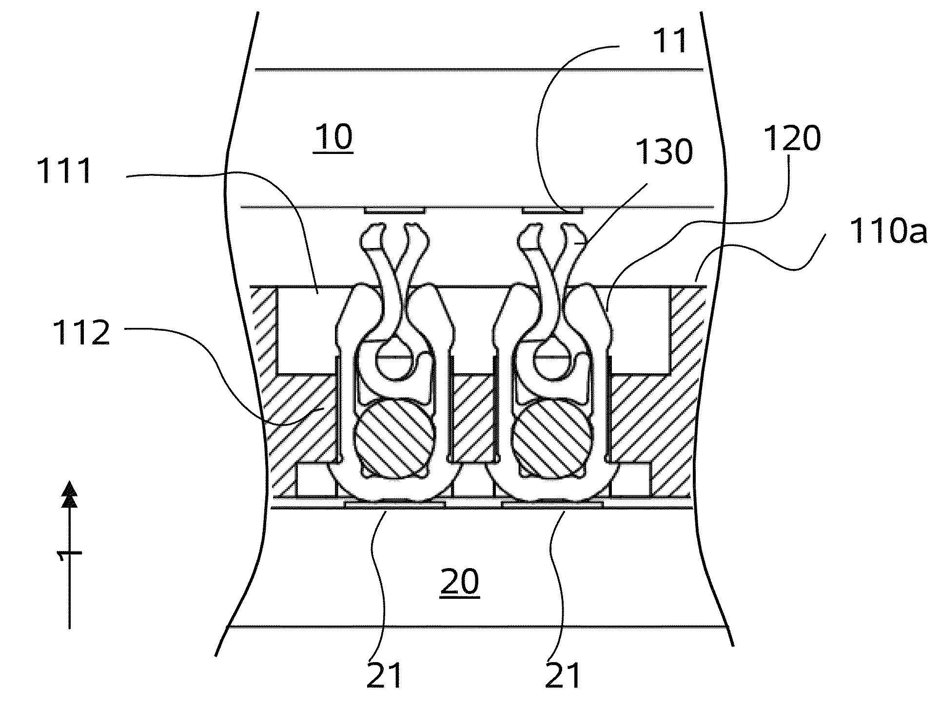
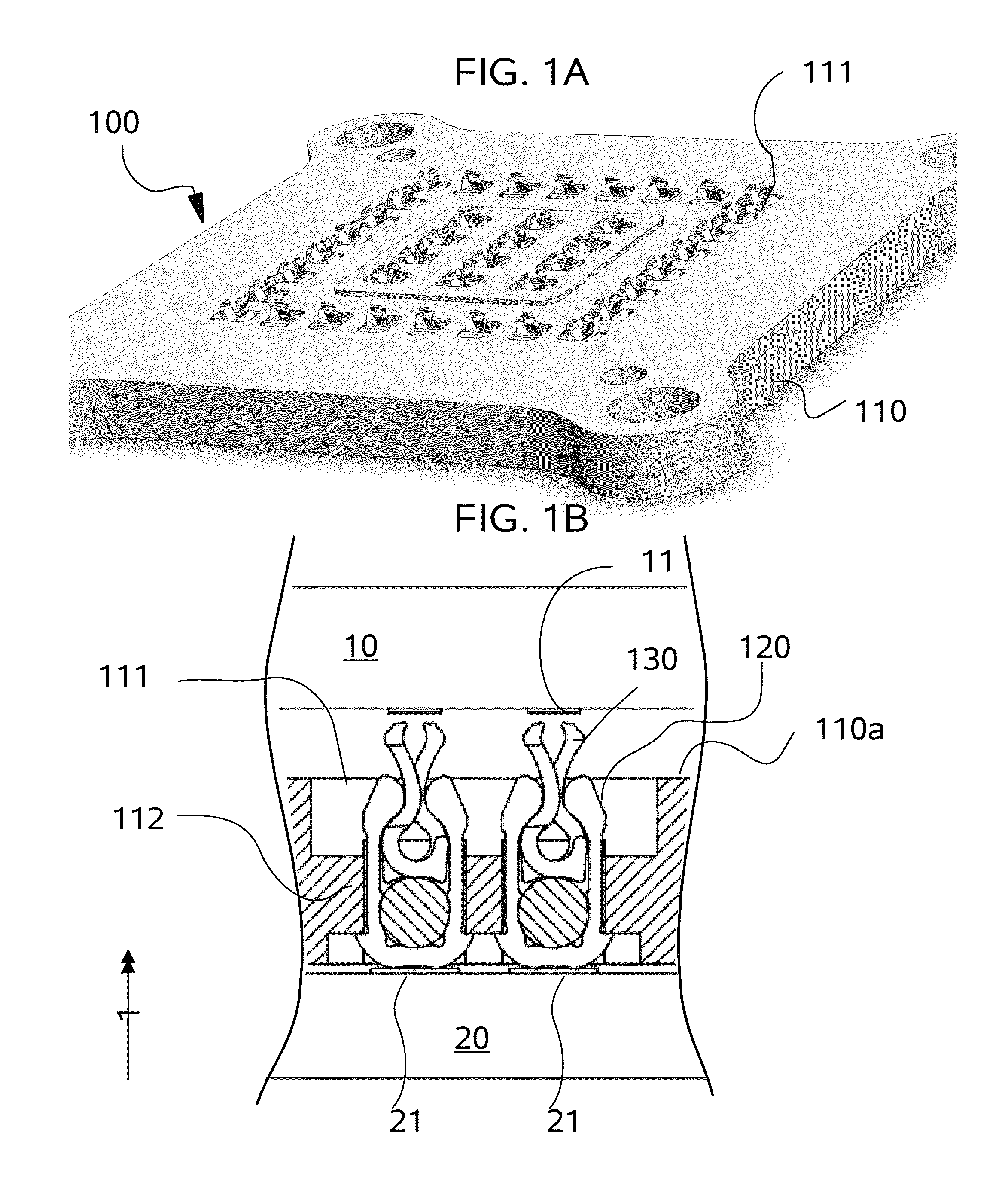
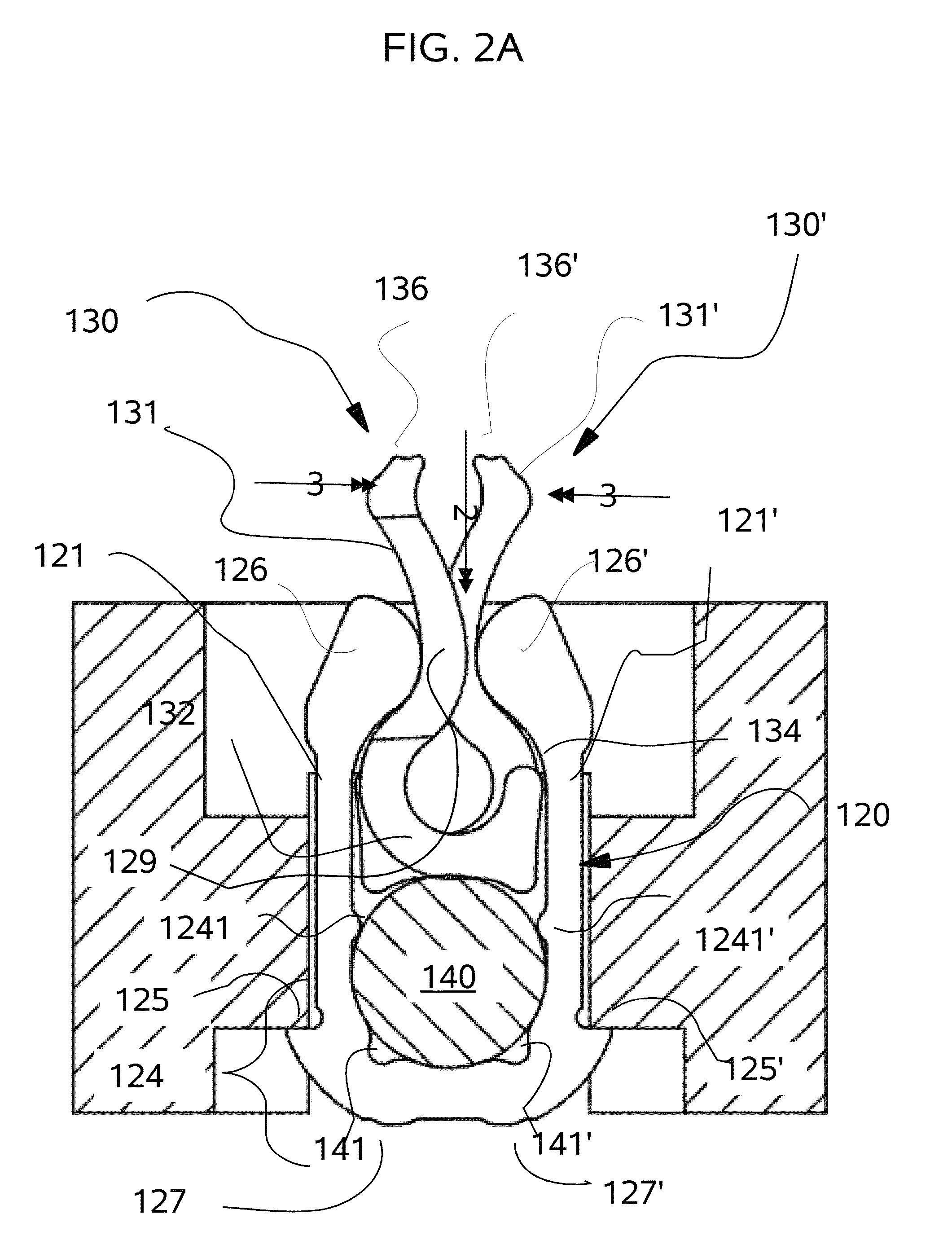
[0046]Referring to FIGS. 1 through 18, wherein like reference numerals refer to like components in the various views, there is illustrated therein a new and improved Electronic Device Test Fixture, generally denominated 100 herein.
[0047]Electronic device test fixtures commonly deploy a plurality of contact elements in a dielectric housing (or holder) to coincide with the microcircuits' terminal locations. The contact elements are able to make repeated electrical connections with thousands of DUT's at the upper side of the test fixture to conduct signals to the test circuit board of the instrument test head platform generally below.
[0048]In accordance with the present invention, FIG. 1A illustrates a general embodiment of the test fixture 100 that comprises a housing 110 with a plurality of cavities 111. The test fixture 100 is disposed between test board 20 that has a series of terminals 21 and the DUT 10 with its series of pads 11 or other exposed external electrical terminals or c...
PUM
 Abstract
Description
Claims
Application Information