Integrated circuit package with overlapping bond fingers

a technology of integrated circuits and fingers, which is applied in the direction of solid-state devices, basic electric elements, electrical apparatus construction details, etc., can solve the problems of not being able to adopt the ics wholesale technology, the density of connections cannot keep up with the constant shrinkage of dimensions of integrated circuit chips, and the difficulty of adapting the sub-microscopic dimensions of integrated circuit technology to the macroscopic environmen

Inactive Publication Date: 2005-10-18
INT BUSINESS MASCH CORP
View PDF17 Cites 13 Cited by
  • Summary
  • Abstract
  • Description
  • Claims
  • Application Information

AI Technical Summary

Benefits of technology

[0013]Another aspect of the invention is that the overlap areas permit a set of bond pads to take up less distance along the transverse axis, so that more pads can be placed within a bond pad module.

Problems solved by technology

In the field of packaging integrated circuits, a recurring problem has been that of increasing the density of connections to keep up with the constant shrinkage of dimensions on the integrated circuit chips.
Packaging technology has not been able to adopt the technology of ICs wholesale for a number of reasons, including cost and the difficulty of adapting the sub-microscopic dimensions of integrated circuit technology to the macroscopic environment in which packages operate.
It also suffers from increased inductance due to relatively long bond wires.

Method used


Image

  • Integrated circuit package with overlapping bond fingers
  • Integrated circuit package with overlapping bond fingers
  • Integrated circuit package with overlapping bond fingers

Examples


Embodiment Construction

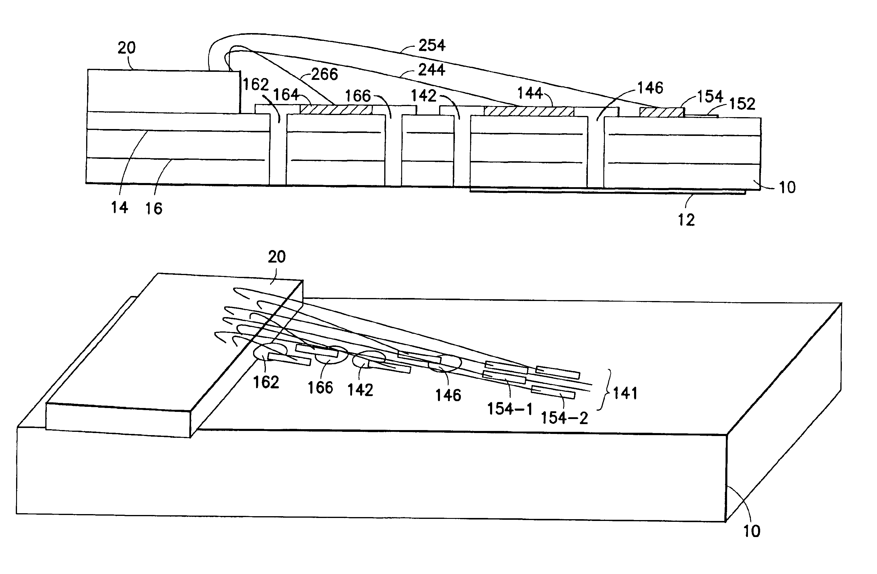
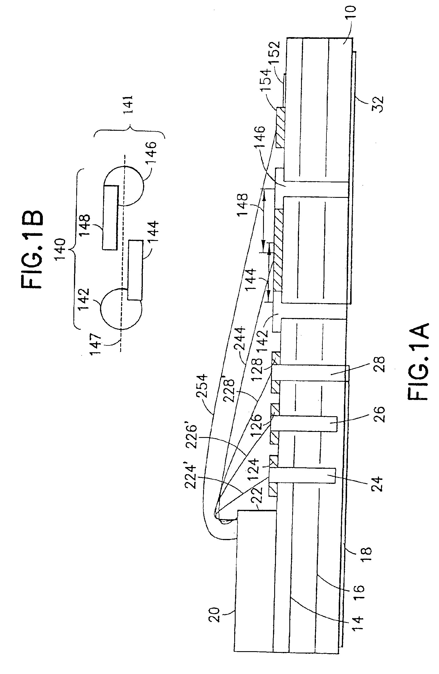
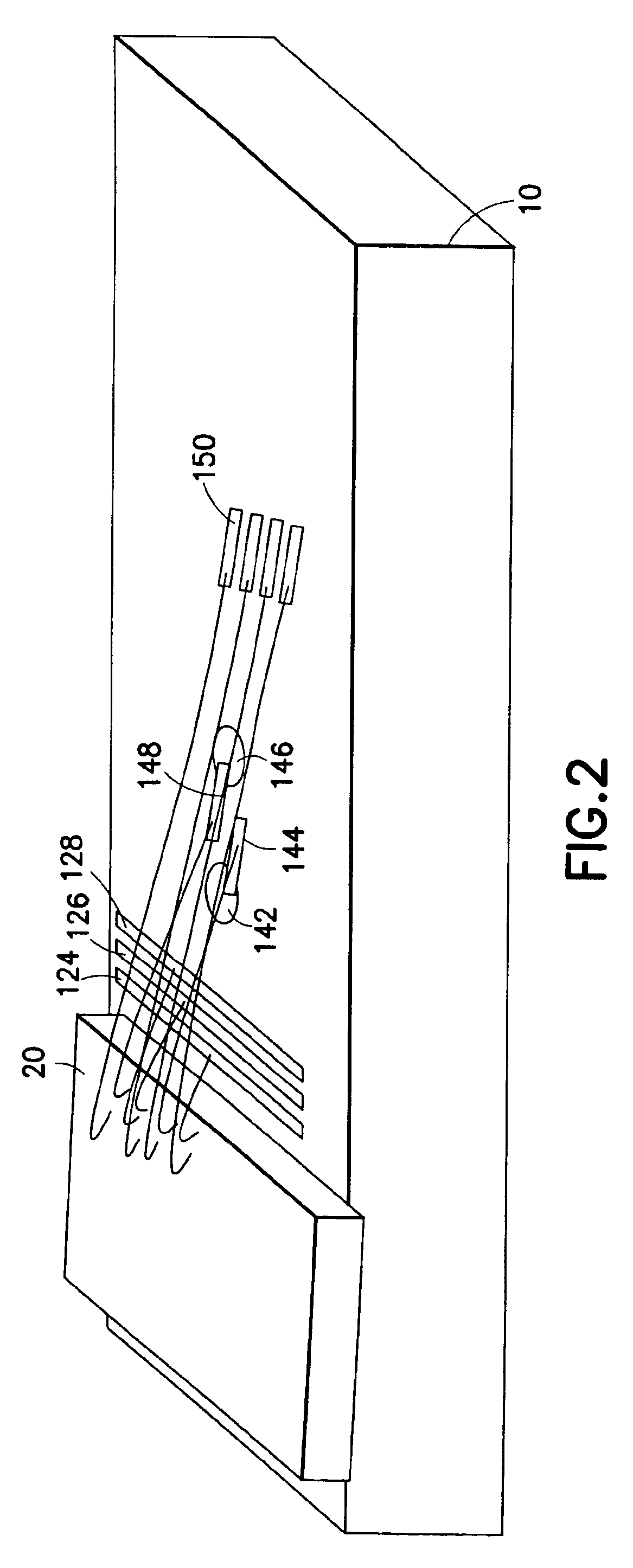
[0024]FIG. 1A shows a cross section of an embodiment of the invention, in which substrate 10 is the base layer of a package. Substrate 10 contains power planes 14, 16 and 18 embedded in it or on the bottom surface to carry ground, Vdd and another voltage level around to various places where the power can be tapped into die 20. Three power rings, 124, 126 and 128 are connected by vias 24, 26 and 28 respectively, to the power planes 14, 16 and 18, respectively. The rings are connected by bond wires 224′, 226′ and 228′ to connections on die 20.

[0025]On the same level, vias 142 and 146 carry signals passing to and from the die and signal bond pads 144 and 148 (also referred to as bond fingers) on wire 244 and a corresponding wire behind wire 244. The vias are connected to a network of signal connectors represented schematically by heavy line 32 on the bottom of substrate 10. Signal lines could also be formed on the top surface or at an intermediate height location if space allows.

[0026]...


PUM


Abstract

An integrated circuit package comprises a set of bond fingers for connecting wire bonds from the chip, the bond fingers being placed overlapping on a transverse axis from the chip and extending inwardly and outwardly from vias positioned at different positions along the transverse axis, so that wire bonds connected to adjacent fingers have the same length.

Description

TECHNICAL FIELD[0001]The field of the invention is that of packaging integrated circuits.BACKGROUND OF THE INVENTION[0002]In the field of packaging integrated circuits, a recurring problem has been that of increasing the density of connections to keep up with the constant shrinkage of dimensions on the integrated circuit chips.[0003]Packaging technology has not been able to adopt the technology of ICs wholesale for a number of reasons, including cost and the difficulty of adapting the sub-microscopic dimensions of integrated circuit technology to the macroscopic environment in which packages operate.[0004]In the particular case of wire-bond technology, the mechanical requirements of the wire-bond machines set requirements of strength and thus of dimension on the wires. The dimensional requirements on the wires impose corresponding requirements on the bond pads to which the wires are bonded.[0005]On solution that has been used in the art is to place one or more continuous rings close...

Claims


Application Information

Patent Timeline
Patent Type & Authority Patents(United States)
IPC IPC(8): H01L23/48H01L23/50H01L23/498
CPCH01L23/49838H01L23/50H01L24/49H01L2224/48091H01L2224/48227H01L2224/48235H01L2224/4943H01L2924/01005H01L2924/01006H01L2924/01082H01L2924/14H01L2924/30107H01L2924/00014H01L24/48H01L2924/01033H01L2224/48233H01L2224/49433H01L2224/45099H01L2224/05599H01L2924/00012
Inventor KUZAWINSKI, MARK J.WOLF, EDWARD M.
Owner INT BUSINESS MASCH CORP
Why Eureka
Try Eureka